74HC165(2017) View Datasheet(PDF) - NXP Semiconductors.
Part Name
Description
MFG CO.
74HC165 Datasheet PDF : 22 Pages
| |||
Nexperia
74HC165; 74HCT165
8-bit parallel-in/serial out shift register
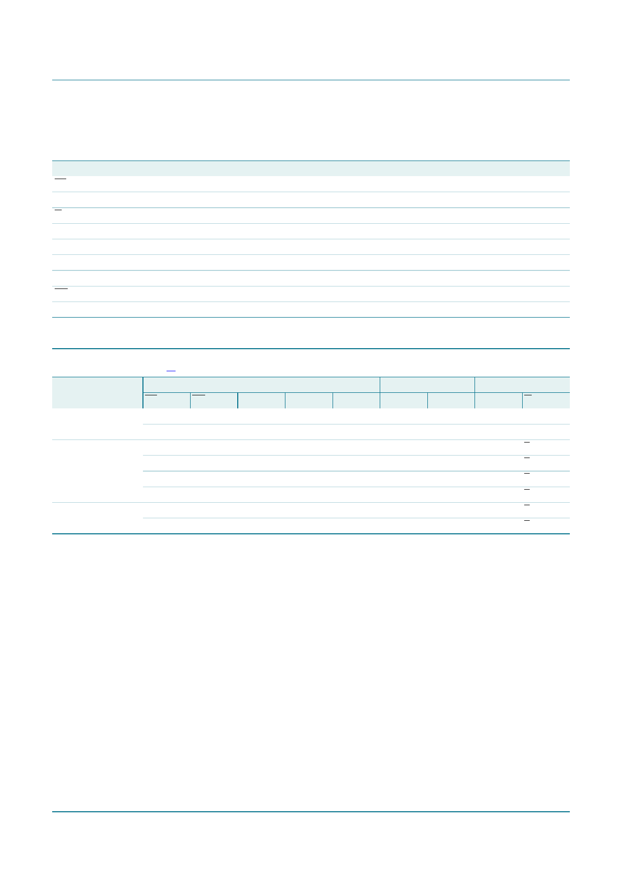
6.2 Pin description
Table 2. Pin description
Symbol
Pin
PL
1
CP
2
Q7
7
GND
8
Q7
9
DS
10
D0 to D7
11, 12, 13, 14, 3, 4, 5, 6
CE
15
VCC
16
Description
asynchronous parallel load input (active LOW)
clock input (LOW-to-HIGH edge-triggered)
complementary output from the last stage
ground (0 V)
serial output from the last stage
serial data input
parallel data inputs (also referred to as Dn)
clock enable input (active LOW)
positive supply voltage
7 Functional description
Table 3. Function table [1]
Operating modes Inputs
Qn registers
Outputs
PL
CE
CP
DS
D0 to D7 Q0
Q1 to Q6 Q7
Q7
parallel load
L
X
X
X
L
L
L to L
L
H
L
X
X
X
H
H
H to H
H
L
serial shift
H
L
↑
l
X
L
q0 to q5 q6
q6
H
L
↑
h
X
H
q0 to q5 q6
q6
H
↑
L
l
X
L
q0 to q5 q6
q6
H
↑
L
h
X
H
q0 to q5 q6
q6
hold "do nothing" H
H
X
X
X
q0
q1 to q6 q7
q7
H
X
H
X
X
q0
q1 to q6 q7
q7
[1] H = HIGH voltage level;
h = HIGH voltage level one set-up time prior to the LOW-to-HIGH clock transition;
L = LOW voltage level;
l = LOW voltage level one set-up time prior to the LOW-to-HIGH clock transition;
q = state of the referenced output one set-up time prior to the LOW-to-HIGH clock transition;
X = don’t care;
↑ = LOW-to-HIGH clock transition.
74HC_HCT165
Product data sheet
All information provided in this document is subject to legal disclaimers.
Rev. 5 — 21 August 2017
© Nexperia B.V. 2017. All rights reserved.
4 / 22
Share Link: 