74ALVC125D View Datasheet(PDF) - Philips Electronics
Part Name
Description
MFG CO.
74ALVC125D Datasheet PDF : 16 Pages
| |||
Philips Semiconductors
Quad buffer/line driver; 3-state
Product specification
74ALVC125
FEATURES
• Wide supply voltage range from 1.65 to 3.6 V
• Complies with JEDEC standard:
JESD8-7 (1.65 to 1.95 V)
JESD8-5 (2.3 to 2.7 V)
JESD8B/JESD36 (2.7 to 3.6 V)
• 3.6 V tolerant inputs/outputs
• CMOS low power consumption
• Direct interface with TTL levels (2.7 to 3.6 V)
• Power-down mode
• Latch-up performance exceeds 250 mA
• ESD protection:
HBM EIA/JESD22-A114-A exceeds 2000 V
MM EIA/JESD22-A115-A exceeds 200 V.
DESCRIPTION
The 74ALVC125 is a high-performance, low-power,
low-voltage, Si-gate CMOS device and superior to most
advanced CMOS compatible TTL families.
Schmitt-trigger action at all inputs makes the circuit
tolerant for slower input rise and fall times.
The 74ALVC125 consists of four non-inverting buffer/line
drivers with 3-state outputs. The 3-state outputs (nY) are
controlled by the output enable input (nOE). A HIGH on
pin nOE causes the outputs to assume a high-impedance
OFF-state.
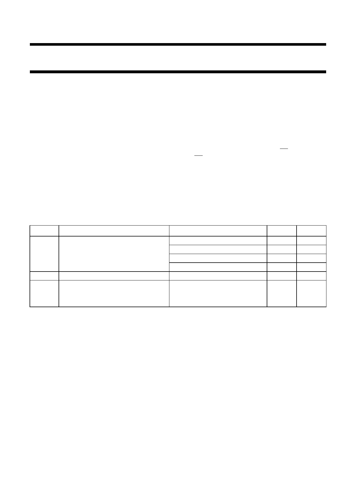
QUICK REFERENCE DATA
GND = 0 V; Tamb = 25 °C.
SYMBOL
PARAMETER
tPHL/tPLH propagation delay inputs nA to output nY
CI
input capacitance
CPD
power dissipation capacitance per buffer
CONDITIONS
VCC = 1.8 V; CL = 30 pF; RL = 1 kΩ
VCC = 2.5 V; CL = 30 pF; RL = 500 Ω
VCC = 2.7 V; CL = 50 pF; RL = 500 Ω
VCC = 3.3 V; CL = 50 pF; RL = 500 Ω
VCC = 3.3 V; notes 1 and 2
outputs enable
outputs disabled
TYPICAL UNIT
2.4
ns
1.7
ns
2.0
ns
1.8
ns
3.5
pF
27
pF
5
pF
Notes
1. CPD is used to determine the dynamic power dissipation (PD in µW).
PD = CPD × VCC2 × fi × N + Σ(CL × VCC2 × fo) where:
fi = input frequency in MHz;
fo = output frequency in MHz;
CL = output load capacitance in pF;
VCC = supply voltage in Volts;
N = total switching outputs;
Σ(CL × VCC2 × fo) = sum of the outputs.
2. The condition is VI = GND to VCC.
2002 Nov 18
2
Share Link: 