74AHCT1G04 View Datasheet(PDF) - Philips Electronics
Part Name
Description
MFG CO.
74AHCT1G04 Datasheet PDF : 16 Pages
| |||
Philips Semiconductors
Inverter
AC WAVEFORMS
Product specification
74AHC1G04; 74AHCT1G04
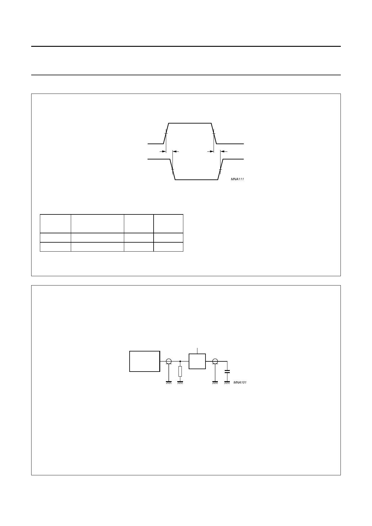
handbook, halfpage
A input
Y output
VM
tPHL
VM
tPLH
MNA111
FAMILY
AHC1G
AHCT1G
VI INPUT
VM
VM
REQUIREMENTS INPUT OUTPUT
GND to VCC
GND to 3.0 V
50% VCC 50% VCC
1.5 V
50% VCC
Fig.5 Input (A) to output (Y) propagation delays.
handbook, halfpage
VI
PULSE
GENERATOR
VCC
VO
D.U.T.
RT
CL
MNA101
Definitions for test circuit:
CL = load capacitance including jig and probe capacitance (see Chapter “AC characteristics”).
RT = termination resistance should be equal to the output impedance Z0 of the pulse generator.
Fig.6 Load circuitry for switching times.
2002 May 27
8
Share Link: 