EN29F002N(2000) View Datasheet(PDF) - Eon Silicon Solution Inc.
Part Name
Description
MFG CO.
EN29F002N Datasheet PDF : 32 Pages
| |||
SWITCHING WAVEFORMS (continued)
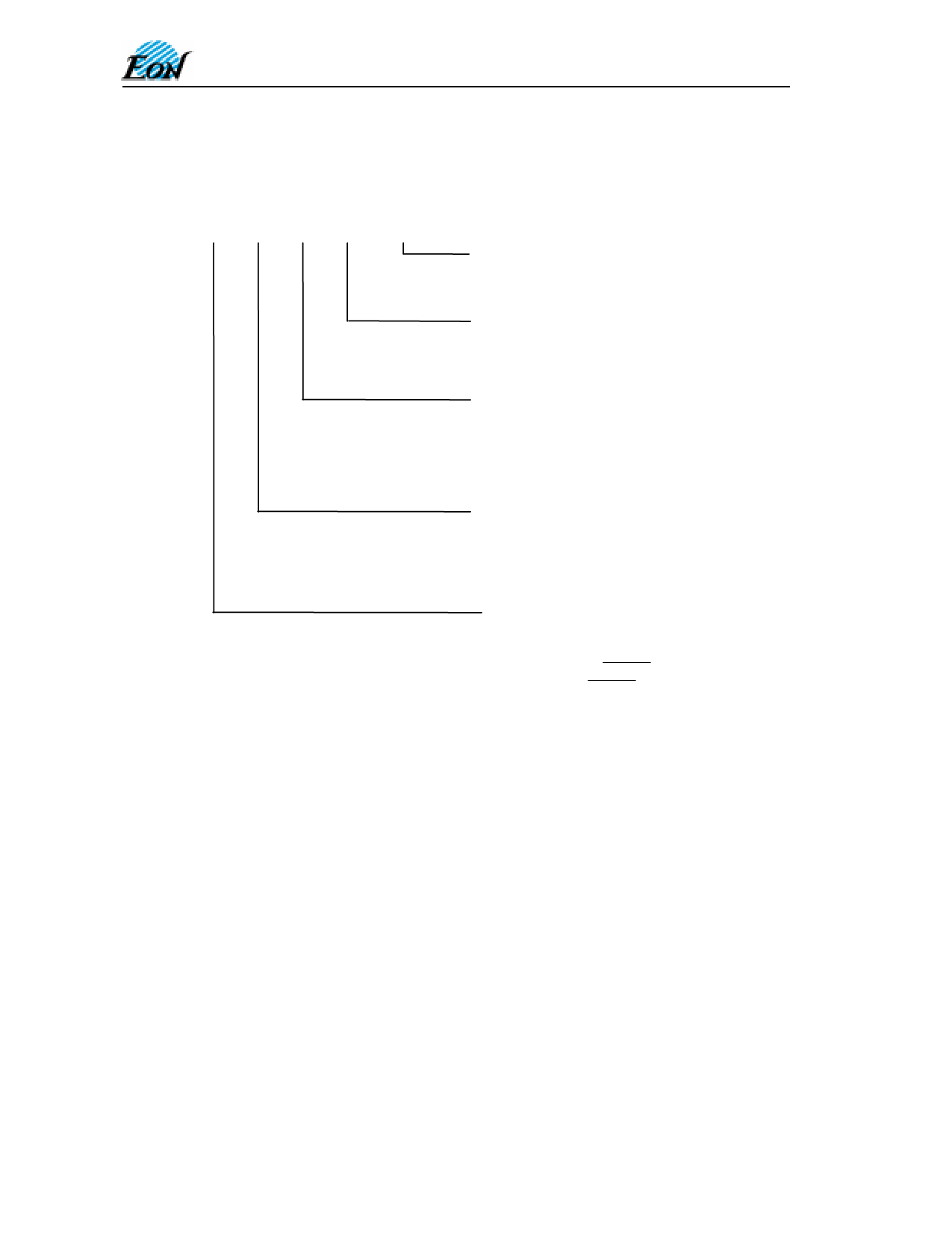
Figure 11. /RESET Timing Diagram
EN29F002 / EN29F002N
Figure 12. Alternate /CE Controlled Write Operation Timings
Notes:
1. PA is address of the memory location to be programmed.
2. PD is data to be programmed at byte address.
3. /DQ7 is the output of the complement of the data written to the device.
4. DOUT is the output of data written to the device.
5. Figure indicates last two bus cycles of four bus cycle sequence.
4800 Great America Parkway, Suite 202
31
Santa Clara, CA 95054
Tel: 408-235-8680
Fax: 408-235-8685
Share Link: 