UPD16314GJ-002-8EU View Datasheet(PDF) - NEC => Renesas Technology
Part Name
Description
MFG CO.
UPD16314GJ-002-8EU
NEC => Renesas Technology
UPD16314GJ-002-8EU Datasheet PDF : 48 Pages
| |||
µ PD16314
3.2 Logic system (Microprocessor Interface)
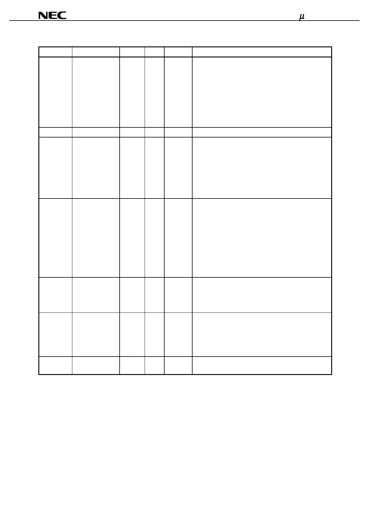
Pin Symbol
Pin Name
Pin No. I/O
RS,STB
Register
select/strobe
13
I
/CS
Chip select
26
I
E(/RD),
Enable(read)/shift
14
I
SCK
clock
R,/W(/WR) Read/write signal
12
I
(write)
SI,SO
Serial I/O
15
I/O
DB0 - DB7 Parallel data I/O 16 to 23 I/O
/RESET
Reset
7
I
Output
CMOS-
3-states
CMOS-
3-states
Description
When Parallel data transfer is selected, this pin is Register
select.
L: Select instruction register(IR).
H: Select data register(DR).
When serial data transfer mode is selected, this pin is the
strobe input. Data can be input when this signal goes L.
Command processing is performed at the rising edge of this
signal.
When this pin is L, this device is active.
When M68 parallel data transfer mode is selected (E), this
pin is enabled. Data is written at the falling edge.
When i80 parallel data transfer selected (/RD), this pin is a
read-enable pin. When this pin is L, data is output to the
data bus.
When serial data transfer is selected, this pin is the shift
clock input. Data is written at the rising edge.
When M68 parallel data transfer mode is selected (R,/W),
this pin is the data transfer select pin.
L: Write
H: Read
When i80 parallel data transfer mode is selected (/WR), this
pin is written a write-enable pin. Data is written at rising
edge of this signal.
When serial data transfer mode is selected this pin is fixed
to H or L.
When serial data transfer mode is selected, this pin is used
as an I/O pin.
When parallel data transfer mode is selected, this pin is
fixed to H or L. DB0 to DB7
When parallel data transfer mode is selected, these pins
are used as I/O pins.
When 4-bits transfer mode is selected, DB4 to DB7 are
used. Data is transferred starting from the most significant
bit (MSB) and stored sequentially.
L: Initializes all the internal registers and commands.
Anode and grid outputs are fixed to VSS2.
Data Sheet S13231EJ1V0DS00
5
Share Link: 