MAX8660BETL(2009) View Datasheet(PDF) - Maxim Integrated
Part Name
Description
MFG CO.
MAX8660BETL
(Rev.:2009)
(Rev.:2009)
Maxim Integrated
MAX8660BETL Datasheet PDF : 43 Pages
| |||
High-Efficiency, Low-IQ, PMICs with Dynamic
Voltage Management for Mobile Applications
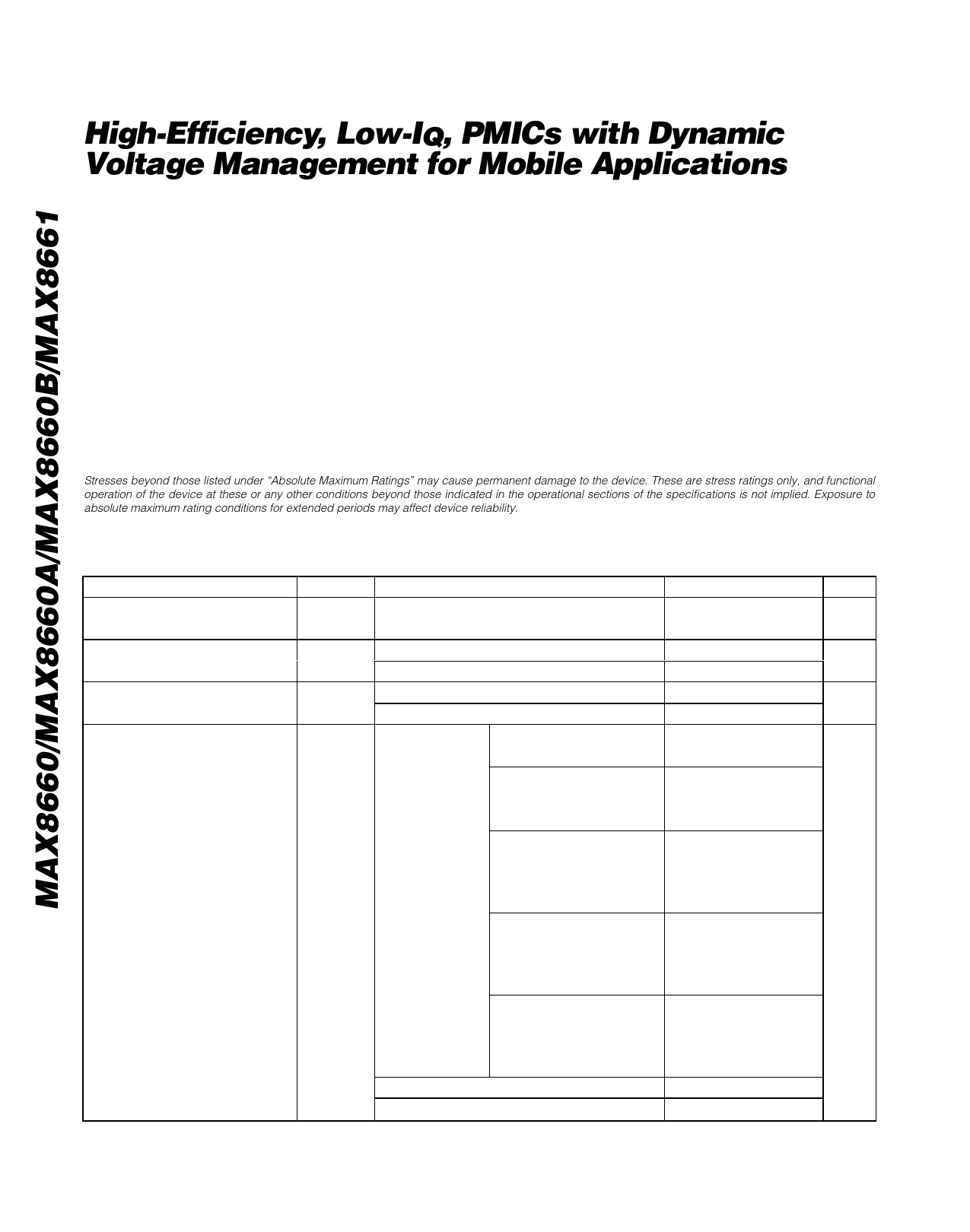
ABSOLUTE MAXIMUM RATINGS
IN, IN5, IN6, IN67, EN2, EN34, EN5, LBO, RSO, MR, SET1,
SET2, V1, V2, V3, V4, SCL, SDA,
SRAD to AGND..................................................-0.3V to +7.5V
LBF, LBR, EN1, RAMP to AGND .................-0.3V to (VIN + 0.3V)
V8 to AGND................................................-0.3V to (VIN8 + 0.3V)
V5 to AGND................................................-0.3V to (VIN5 + 0.3V)
V6, V7 to AGND........................................-0.3V to (VIN67 + 0.3V)
PV1 to PG1 ............................................................-0.3V to +7.5V
PV2 to PG2 ............................................................-0.3V to +7.5V
PV3 to PG3 ............................................................-0.3V to +7.5V
PV4 to PG4 ............................................................-0.3V to +7.5V
PV, PV1, PV2, PV3, PV4, IN8 to IN ........................-0.3V to +0.3V
LX1 Continuous RMS Current (Note 1) .................................2.3A
LX2 Continuous RMS Current (Note 1) .................................2.0A
LX3 Continuous RMS Current (Note 1) .................................2.6A
LX4 Continuous RMS Current (Note 1) .................................1.0A
PG1, PG2, PG3, PG4, EP to AGND.......................-0.6V to +0.6V
GND to AGND ......................................................-0.3V to +0.3V
All REGx Output Short-Circuit Duration......................Continuous
Continuous Power Dissipation (TA = +70°C)
40-Pin Thin QFN (derate 35.7mW/°C above +70°C).....2857mW
Operating Temperature Range ...........................-40°C to +85°C
Junction Temperature ......................................................+150°C
Storage Temperature Range .............................-65°C to +150°C
Lead Temperature (soldering, 10s) .................................+300°C
Note 1: LX_ has internal clamp diodes to PG_ and PV_. Applications that forward bias these diodes must take care not to exceed
the IC’s package power-dissipation limits.
Stresses beyond those listed under “Absolute Maximum Ratings” may cause permanent damage to the device. These are stress ratings only, and functional
operation of the device at these or any other conditions beyond those indicated in the operational sections of the specifications is not implied. Exposure to
absolute maximum rating conditions for extended periods may affect device reliability.
ELECTRICAL CHARACTERISTICS
(VIN = VIN5 = VIN67 = VIN8 = 3.6V, Figure 3, TA = -40°C to +85°C, unless otherwise noted. Typical values are at TA = +25°C.) (Note 2)
PARAMETER
PV1, PV2, PV3, PV4, IN, IN8
Supply Voltage Range
IN Undervoltage-Lockout
Threshold
IN Overvoltage-Lockout
Threshold
SYMBOL
CONDITIONS
VIN
PV1, PV2, PV3, PV4, IN, and IN8 must be
connected together externally
VUVLO
VOVLO
VIN rising
VIN falling
VIN rising
VIN falling
Only V8 on (deep-sleep
power mode)
MIN TYP MAX UNITS
2.6
6.0
V
2.250 2.400 2.550
V
2.200 2.350 2.525
6.20 6.35 6.50
V
6.00 6.15 6.30
20
V1, V2, and V8 on;
V1 and V2 in normal (skip)
50
operating mode
Input Current
V1, V2, V5, and V8 on
IIN+
No load;
IPV1+IPV2+ SDA = SCL = V8
(sleep power mode);
V1 and V2 in normal (skip)
operating mode
90
IPV3+IPV4+
V1, V2, V3, V4, V5, and V8 on
µA
IIN5+
IIN67+ IIN8
(run power mode);
V1, V2, V3, and V4 in normal
140
(skip) operating mode
V1, V2, V3, V4, V5, V6, V7,
and V8 (all on);
V1, V2, V3, and V4 in normal
250
(skip) operating mode
Undervoltage lockout, VIN = 2.2V
1.5
Overvoltage lockout, VIN = 6.5V
25
4 _______________________________________________________________________________________
Share Link: 