HY27SS08561M-TP View Datasheet(PDF) - Hynix Semiconductor
Part Name
Description
MFG CO.
HY27SS08561M-TP Datasheet PDF : 44 Pages
| |||
HY27SS(08/16)561M Series
HY27US(08/16)561M Series
256Mbit (32Mx8bit / 16Mx16bit) NAND Flash
RB
I/O
00h/
01h/50h
Command
Code
tBLBH1
(Read Busy time)
tBLBH1
tBLBH1
Busy
Address Inputs
1st
Page Output
Busy
2nd
Page Output
Busy
Nth
Page Output
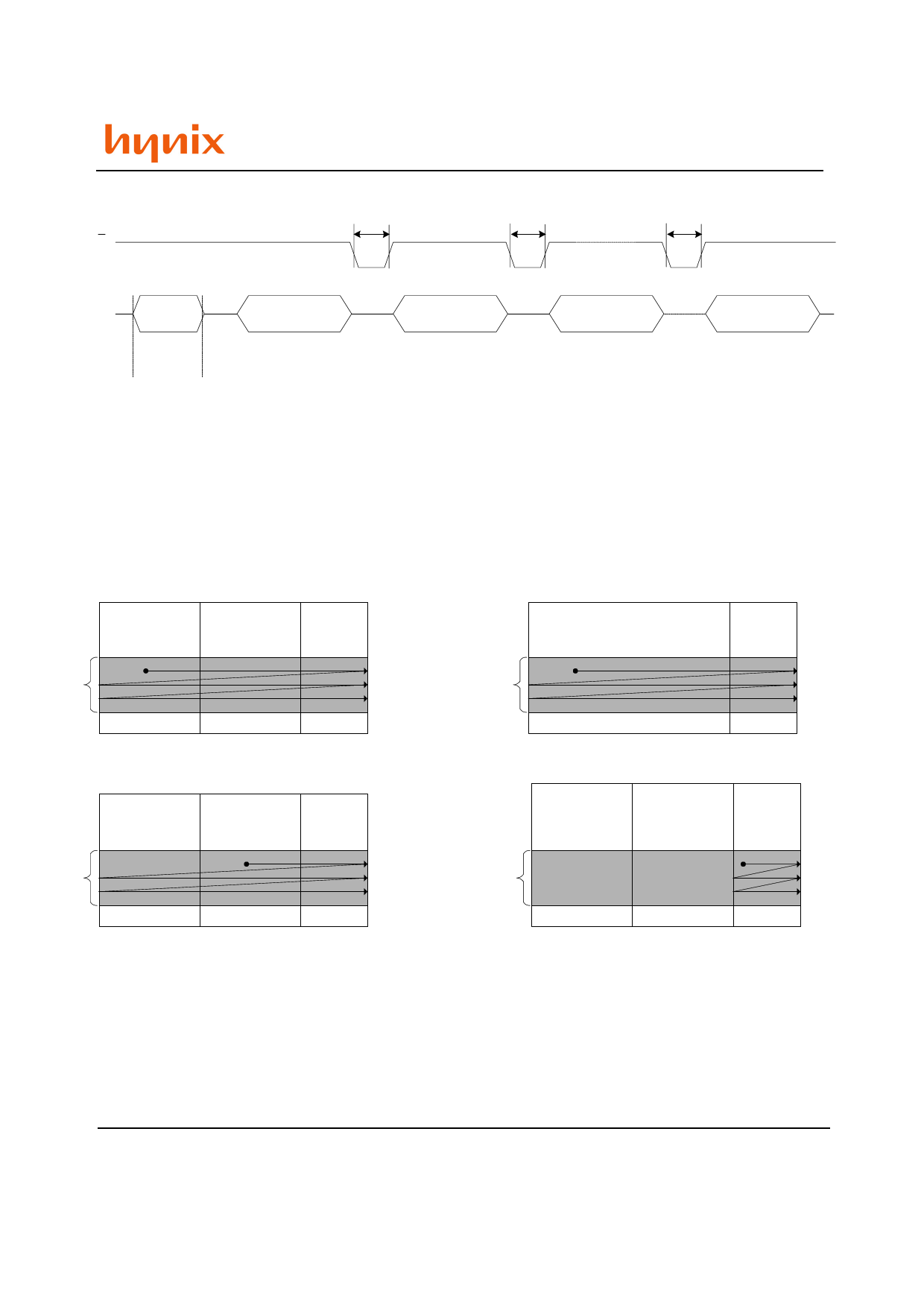
Figure 12. Sequential Row Read Operation
Block
Read A Command, x8 Devices
Area A
(1st half Page)
Area B
(2nd half
Page)
Area C
(Spare)
1st Page
2nd Page
Nth Page
Block
Read A Command, x16 Devices
Area A
(main area)
Area C
(50h)
1st Page
2nd Page
Nth Page
Note : GND input=L, 00h Command
Block
Read B Command, x8 Devices
Area A
(1st half Page)
Area B
(2nd half
Page)
Area C
(Spare)
1st Page
2nd Page
Nth Page
Note : GND input=L, 00h Command
Read C Command, x8/x16 Devices
Area A
Area A/B
Area C
(Spare)
Block
1st Page
2nd Page
Nth Page
Note : GND input=L, 01h Command
Note : GND input=L, 50h Command
Figure 13. Sequential Row Read Block Diagrams
Rev 0.7 / Oct. 2004
16
Share Link: 