PI74ALVTC16374 View Datasheet(PDF) - Pericom Semiconductor Corporation
Part Name
Description
MFG CO.
PI74ALVTC16374 Datasheet PDF : 9 Pages
| |||
PI74ALVTC16374
16-Bit D-Type Flip-Flop
with 3-State Outputs 1122334455667788990011223344556677889900112233445566778899001122112233445566778899001122334455667788990011223344556677889900112211223344556677889900112233445566778899001122334455667788990011221122334455667788990011223344556677889900112233445566778899001122112233445566778899001122
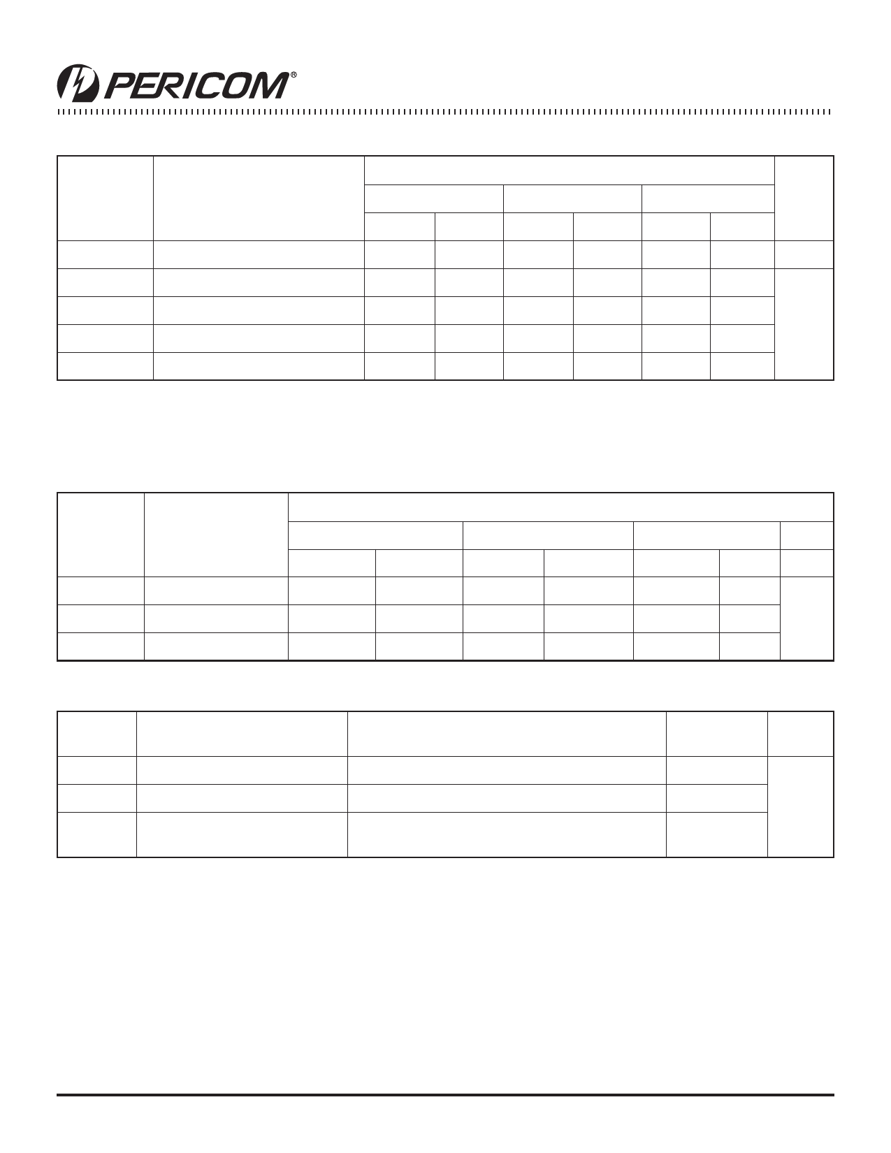
AC Electrical Characteristics
Symbol
Parameter
TA = –40°C to +85°C, CL = 50pF, RL = 500Ω
VDD = 3.3V ±0.3V VDD = 2.5V ±0.2V
VDD = 1.8V
Min. Max. Min. Max. Min. Max.
Units
fMAX
Maximum Clock Frequency
250
250
250
MHz
tPLH, tPHL
Prop Delay, CLK to Q
1.0
3.2
1.5
4.2
1.5
4.8
tPZH, tPZL
tPHZ, tPLZ
Output Enable Time
Output Disable Time
1.0
3.2
1.0
4.7
1.5
5.0
ns
1.0
3.4
1.0
3.8
1.5
4.0
tOSHL, tOSLH Output to Output Skew(1)
0.5
0.5
0.5
Notes:
1. Skew is defined as the absolute value of the difference between the actual propagation delay for any two separate outputs of the same
device. The specification applies to any outputs switching in the same direction, either HIGH or LOW (tOSHL)or LOW to HIGH (tOSLH).
AC Setup Requirements
Symbol
Parameter
tSU
Setup Time
tH
Hold Time
tW
Pulse Width
TA = –40ºC to +85ºC, CL = 50pF, RL = 500Ω
VDD =3.3V ± 0.3V
VDD =2.5V ± 0.2V
VDD =1.8V
Min.
Typ.
Min.
Typ.
Min.
Typ.
1.0
1.0
1.0
0.5
0.5
1.0
1.5
1.5
1.5
Units
ns
Capacitance
Symbol
CIN
COUT
Parameter
Input Capacitance
Output Capacitance
CPD Power Dissipation Capacitance
Conditions
VDD = 1.8, 2.5V or 3.3V, VI = 0V or VDD
VI = 0V or VDD, VDD = 1.8V, 2.5V or 3.3V
VI = 0V or VDD, F = 10 MHz
VDD = 1.8V, 2.5V or 3.3V
TA = +25°C
Typical
6
7
20
Units
pF
7
PS8356C 11/06/08
Share Link: 