MK2011STR View Datasheet(PDF) - Integrated Circuit Systems
Part Name
Description
MFG CO.
MK2011STR Datasheet PDF : 4 Pages
| |||
I CR O C LOC K
MK2011
Fast Ethernet Clock Source
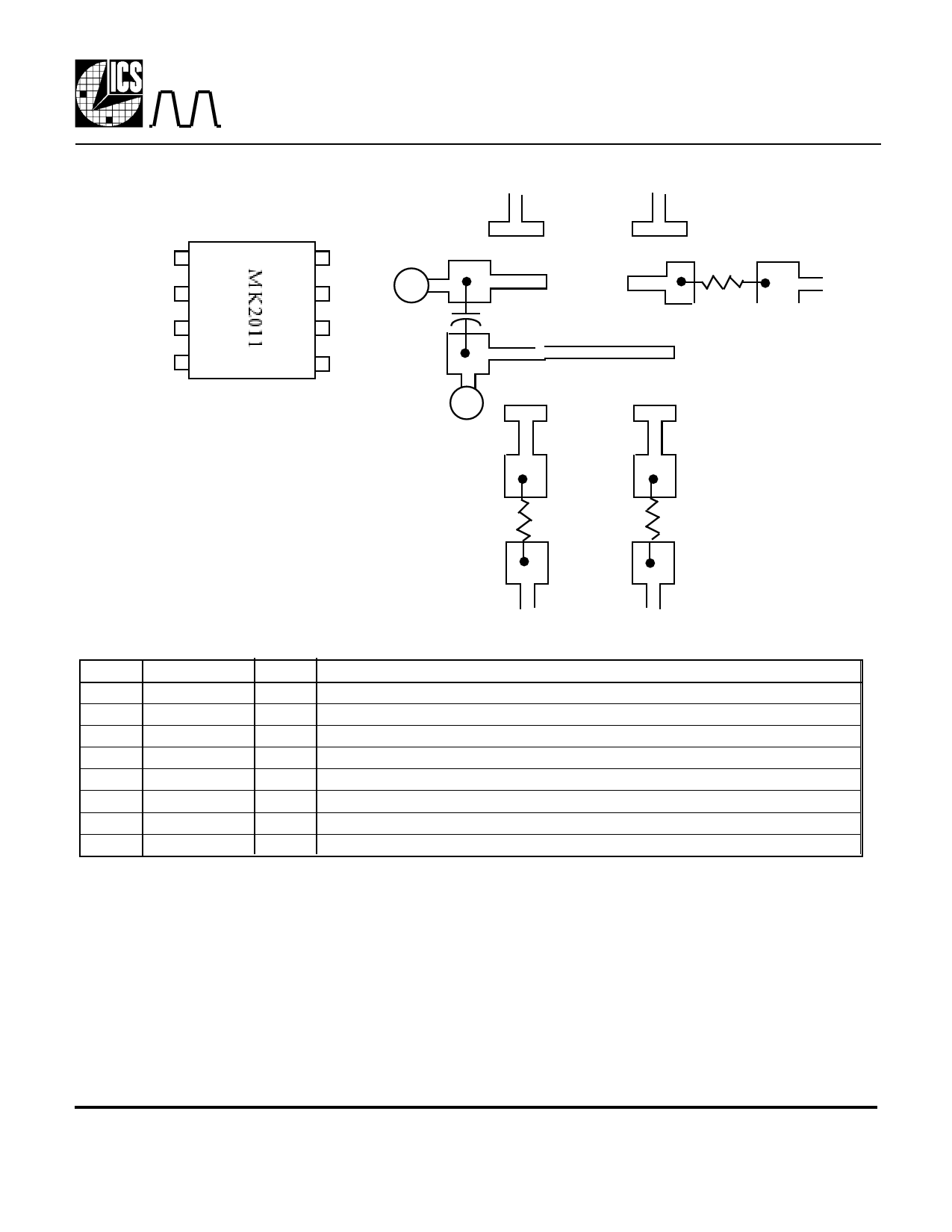
Pin Assignment
X1/ICLK 1
VDD 2
GND 3
25M 4
Suggested Layout
20.00 MHz in
(crystal caps not
shown)
Pin 1 8
8 X2
7 20M V
2
7
6 GND 0.1µF
3
6
5 50M
20MHz
out
33Ω (optional)
8 pin SOIC
G
4
5
33Ω (optional)
33Ω (optional)
Pin Descriptions
25MHz out 50MHz out
Number
1
2
3
4
5
6
7
8
Name
X1/ICLK
VDD
GND
25M
50M
GND
20M
X2
Type
I
P
P
O
O
P
O
O
Description
Crystal Connection. Connect to a 20.000 MHz crystal or clock.
Connect to +5V.
Connect to ground.
25.000 MHz clock output.
50.000 MHz clock output.
Connect to ground.
20.000 MHz buffered crystal clock output.
Crystal Connection to a 20.000 MHz crystal, or leave unconnected for clock input.
Key: I = Input, O = output, P = power supply connection
External Components/Crystal Selection
A minimum number of external components are required for proper oscillation. For a crystal input, one
22pF load capacitor should be connected to each of the X1 and X2 pins and ground, and a parallel
resonant 20.000 MHz, 16pF load, crystal is recommended. The frequency tolerance of the crystal should
be 50ppm or better. For a clock input, connect to X1 and leave X2 unconnected. A decoupling capacitor of
0.1µF should be connected between VDD and GND on pins 2 and 3, and 33Ω terminating resistors
should be used on clock outputs with traces longer than 1 inch.
MDS 2011 B
2
Revision 120597
Printed 11/15/00
MicroClock Division of ICS•1271 Parkmoor Ave.•San Jose•CA•95126•(408)295-9800tel•(408)295-9818fax
Share Link: 