74HC4052DB View Datasheet(PDF) - NXP Semiconductors.
Part Name
Description
MFG CO.
74HC4052DB Datasheet PDF : 29 Pages
| |||
NXP Semiconductors
74HC4052; 74HCT4052
Dual 4-channel analog multiplexer/demultiplexer
Table 10. Dynamic characteristics for 74HCT4052 …continued
GND = 0 V; tr = tf = 6 ns; CL = 50 pF; for test circuit see Figure 15.
Vis is the input voltage at a nYn or nZ terminal, whichever is assigned as an input.
Vos is the output voltage at a nYn or nZ terminal, whichever is assigned as an output.
Symbol Parameter
Conditions
Min
Typ
Max
Unit
Tamb = 40 C to +125 C
tpd
propagation delay Vis to Vos; RL = ; see Figure 13
[2]
VCC = 4.5 V; VEE = 0 V
-
-
18
ns
VCC = 4.5 V; VEE = 4.5 V
ton
turn-on time
E, Sn to Vos; RL = 1 k; see Figure 14
-
-
12
ns
[3]
VCC = 4.5 V; VEE = 0 V
-
-
105
ns
VCC = 4.5 V; VEE = 4.5 V
toff
turn-off time
E, Sn to Vos; RL = 1 k; see Figure 14
-
-
72
ns
[4]
VCC = 4.5 V; VEE = 0 V
-
-
75
ns
VCC = 4.5 V; VEE = 4.5 V
-
-
57
ns
[1] All typical values are measured at Tamb = 25 C.
[2] tpd is the same as tPHL and tPLH.
[3] ton is the same as tPZH and tPZL.
[4] toff is the same as tPHZ and tPLZ.
[5] CPD is used to determine the dynamic power dissipation (PD in W).
PD = CPD VCC2 fi N + {(CL + Csw) VCC2 fo} where:
fi = input frequency in MHz;
fo = output frequency in MHz;
N = number of inputs switching;
{(CL + Csw) VCC2 fo} = sum of outputs;
CL = output load capacitance in pF;
Csw = switch capacitance in pF;
VCC = supply voltage in V.
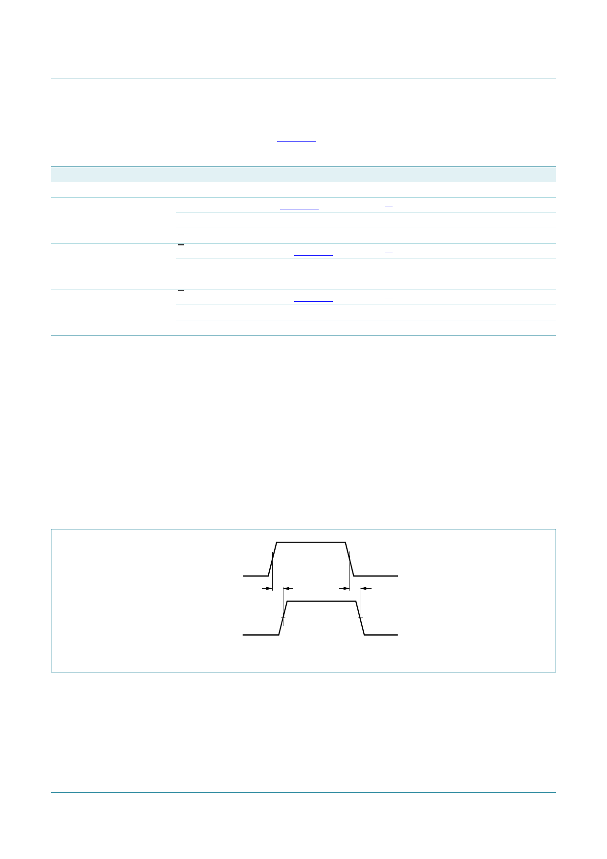
Vis input
Vos output
50 %
tPLH
50 %
Fig 13. Input (Vis) to output (Vos) propagation delays
tPHL
001aad555
74HC_HCT4052
Product data sheet
All information provided in this document is subject to legal disclaimers.
Rev. 10 — 19 July 2012
© NXP B.V. 2012. All rights reserved.
15 of 29
Share Link: 