74LVC1G157 View Datasheet(PDF) - NXP Semiconductors.
Part Name
Description
MFG CO.
74LVC1G157 Datasheet PDF : 15 Pages
| |||
NXP Semiconductors
74LVC1G157
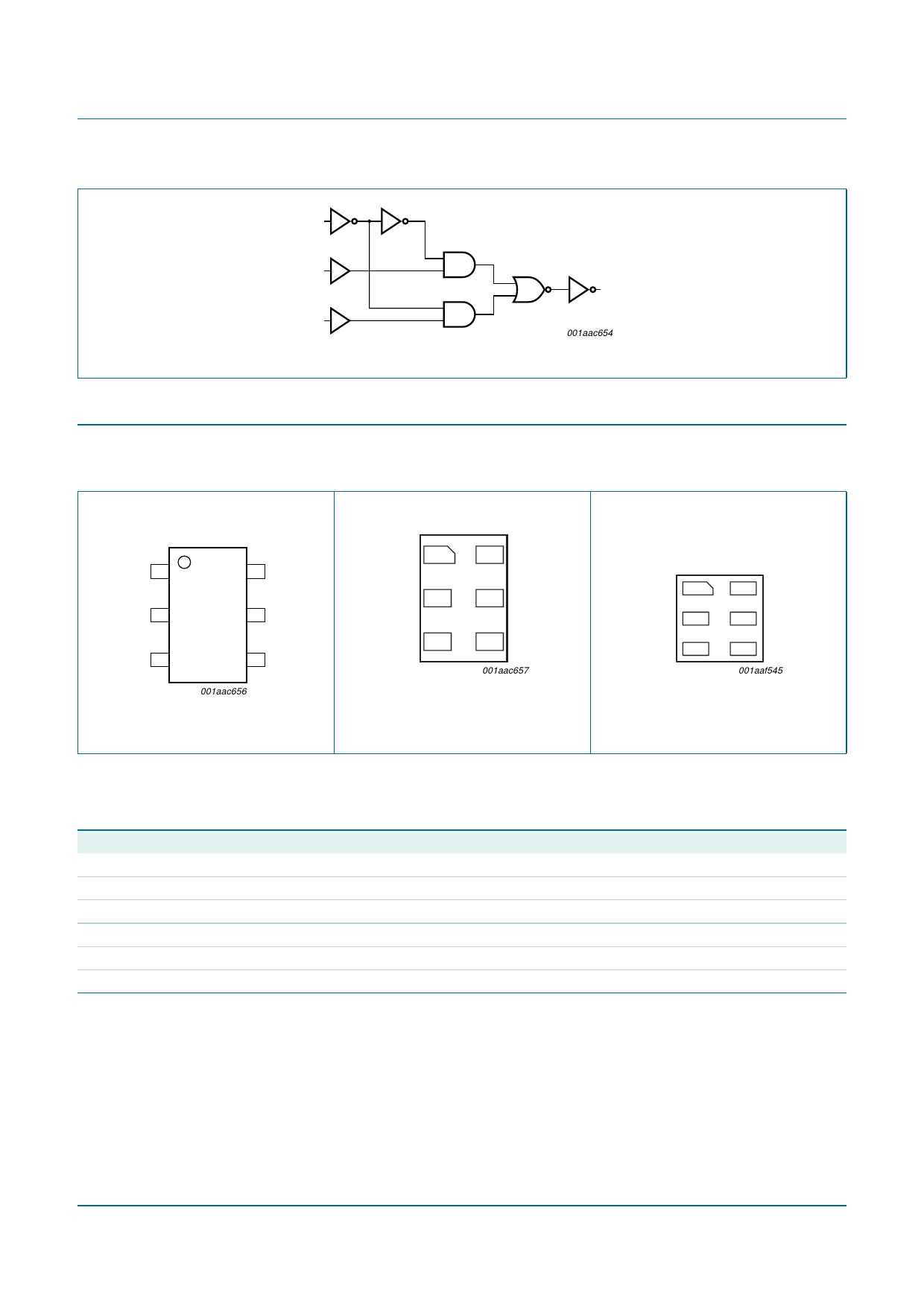
Single 2-input multiplexer
S
I1
I0
Fig 4. Logic diagram
6. Pinning information
6.1 Pinning
Y
001aac654
74LVC1G157
I1 1
6S
GND 2
5 VCC
I0 3
4Y
001aac656
74LVC1G157
I1 1
6S
GND 2
5 VCC
I0 3
4Y
001aac657
Transparent top view
Fig 5. Pin configuration SOT363
Fig 6. Pin configuration SOT886
(SC-88) and SOT457 (SC-74)
(XSON6)
6.2 Pin description
Table 3.
Symbol
I1
GND
I0
Y
VCC
S
Pin description
Pin
1
2
3
4
5
6
Description
data input from source 1
ground (0 V)
data input from source 0
multiplexer output
supply voltage
common data select input
74LVC1G157
I1 1
6S
GND 2
5 VCC
I0 3
4Y
001aaf545
Transparent top view
Fig 7. Pin configuration SOT891
(XSON6)
74LVC1G157_3
Product data sheet
Rev. 03 — 12 July 2007
© NXP B.V. 2007. All rights reserved.
3 of 15
Share Link: 