74LCX374TTR(2004) View Datasheet(PDF) - STMicroelectronics
Part Name
Description
MFG CO.
74LCX374TTR
(Rev.:2004)
(Rev.:2004)
STMicroelectronics
74LCX374TTR Datasheet PDF : 13 Pages
| |||
74LCX374
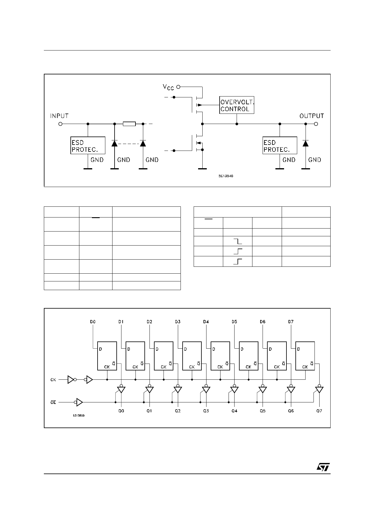
Figure 2: Input And Output Equivalent Circuit
Table 2: Pin Description
PIN N°
1
2, 5, 6, 9, 12,
15, 16, 19
3, 4, 7, 8, 13,
14, 17, 18
11
10
20
SYMBOL
OE
Q0 to Q7
NAME AND FUNCTION
3 State Output Enable
Input (Active LOW)
3-State Outputs
D0 to D7 Data Inputs
CK
GND
VCC
Clock Input (LOW to HIGH,
edge triggered)
Ground (0V)
Positive Supply Voltage
Figure 3: Logic Diagram
Table 3: Truth Table
INPUT
OE
CK
D
H
X
X
L
X
L
L
L
H
X : Don’t Care
Z : High Impedance
OUTPUT
Q
Z
NO CHANGE
L
H
This logic diagram has not be used to estimate propagation delays
2/13
Share Link: 