81C4256A-10 View Datasheet(PDF) - Fujitsu
Part Name
Description
MFG CO.
81C4256A-10 Datasheet PDF : 29 Pages
| |||
Not Recommended for New Design
MB81C4256A-60
MB81C4256A-70
MB81C4256A-80
MB81C4256A-10
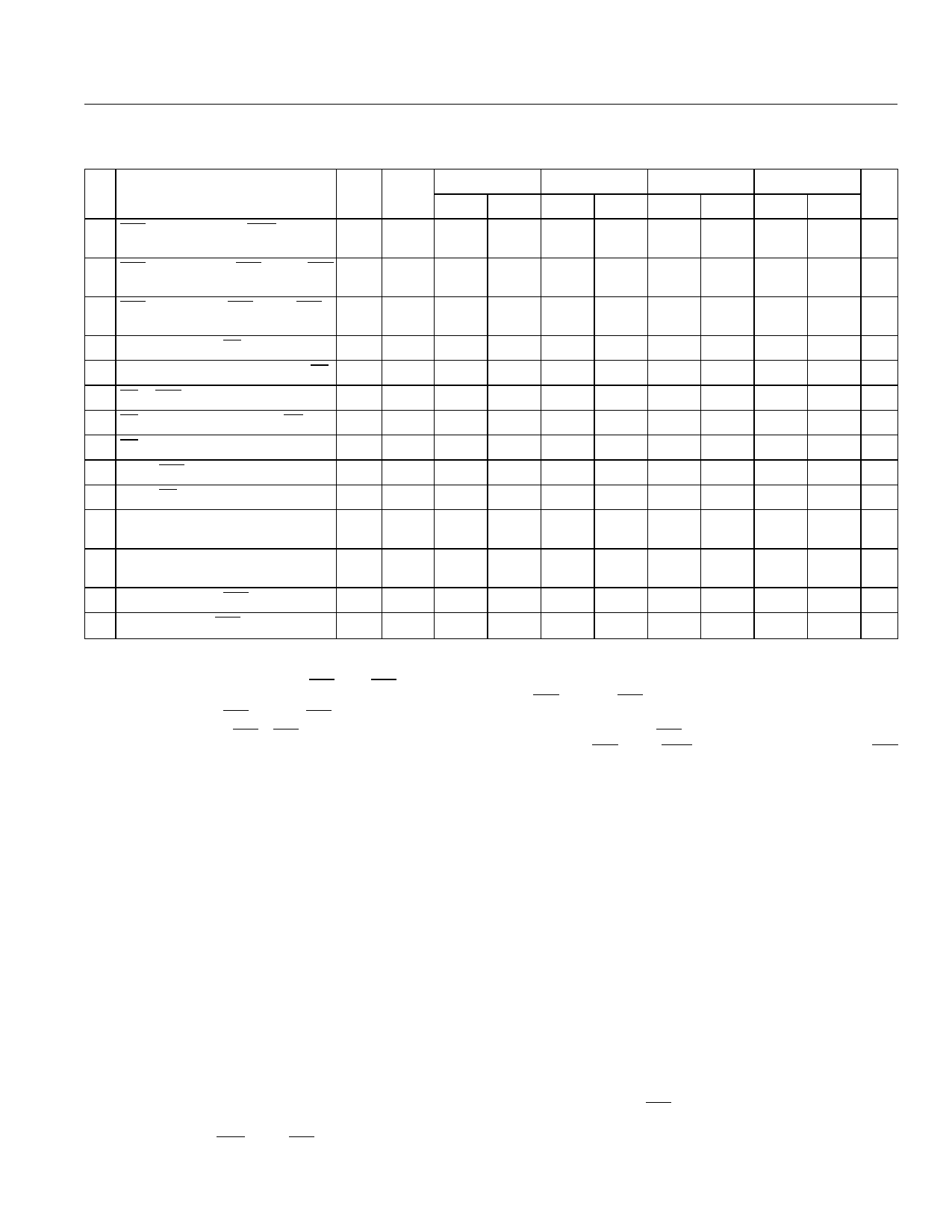
AC CHARACTERISTICS (Continued)
(At recommended operating conditions unless otherwise noted) Notes 3,4,5
MB81C4256A-60 MB81C4256A-70 MB81C4256A-80 MB81C4256A-10
No.
Parameter
Notes Symbol
Unit
Min Max Min Max Min Max Min Max
35
RAS Precharge time to CAS
Active Time (Refresh cycles)
tRPC
0
—
0
—
0
—
0
—
ns
36
CAS Set Up Time for CAS- before-RAS
Refresh
tCSR
0
—
0
—
0
—
0
—
ns
37
CAS Hold Time for CAS-before-RAS
Refresh
tCHR
10
—
10
—
12
—
15
—
ns
38 Access Time from OE
9
tOEA
—
15
—
20
—
20
—
20 ns
39 Output Buffer Turn Off Delay from OE 10
tOEZ
—
15
—
15
—
20
—
25 ns
40 OE to RAS Lead Time for Valid Data
tOEL
10
—
10
—
10
—
10
—
ns
41 OE Hold Time Referenced to WE
16
tOEH
0
—
0
—
0
—
0
—
ns
42 OE to Data In Delay Time
tOED
15
—
15
—
20
—
25
—
ns
43 DIN to CAS Delay Time
17
tDZC
0
—
0
—
0
—
0
—
ns
44 DIN to OE Delay Time
17
tDZO
0
—
0
—
0
—
0
—
ns
50
Fast Page Mode Read/Write Cycle
Time
tPC
40
—
45
—
45
—
50
—
ns
51
Fast Page Mode Read-Modify
Write Cycle Time
tPRWC
77
—
82
—
90
—
110
—
ns
52 Access Time from CAS Precharge
9, 18 tCPA
—
35
—
40
—
40
—
50 ns
53 Fast Page Mode CAS Precharge Time
tCP
10
—
10
—
10
—
10
—
ns
Notes: 1. Referenced to VSS.
2. ICC depends on the output load conditions and cycle rates; The specified values are obtained with the output open. ICC depends on the
number of address change as RAS = VIL, CAS = VlH.
ICC1, ICC3, and ICC5 are specified at one time of address change during RAS = VlL and CAS = VIH. ICC4 is specified at one time of address
change during RAS = VIL and CAS = VIH.
3. An initial pause (RAS = CAS =VIH) of 200 µs is required after power-up followed by any eight RAS-onIy cycles before proper device oper-
ation is achieved. In case of using internal refresh counter, a minimum of eight CAS-before-RAS initialization cycles instead of 8 RAS
cycles are required.
4. AC characteristics assume tT = 5 ns.
5. VlH (min) and VIL (max) are reference levels for measuring timing of input signals. Also, transition times are measured between VIH (min)
and VIL (max).
6. Assumes that tRCD ≤ tRCD (max), tRAD ≤ tRAD (max). If tRCD is greater than the maximum recommended value shown in this table, tRAC will be
increased by the amount that tRCD exceeds the value shown. Refer to Fig. 2 and 3.
7. Assumes that tRCD ≥ tRCD (max), tRAD ≥ tRAD (max). If tASC ≥ tAA - tCAC - tT, access time is tCAC.
8. If tRAD ≥ tRAD (max) and tASC < tAA - tCAC - t T, access time is tAA
9. Measured with a load equivalent to two TTL loads and 100 pF.
10. tOFF and tOEZ is specified that output buffer change to high impedance state.
11. Operation within the tRCD (max) limit ensures that tRAC (max) can be met. tRCD (max) is specified as a reference point only; if tRCD is greater
than the specified tRCD (max) limit, access time is controlled exclusively by tCAC or tAA.
12. tRCD (min) = tRAH (min) + 2t T + tASC (min).
13. Operation within the tRAD (max) limit ensures that tRAC (max) can be met. tRAD (max) is specified as a reference point only; if tRAD is greater
than the specified tRAD (max) limit, access time is controlled exclusively by tCAC or t AA.
14. Either tRRH or tRCH must be satisfied for a read cycle.
15. tWCS is specified as a reference point only. If tWCS ≥ tWCS (min) the data output pin will remain High-Z state through entire cycle.
16. Assumes that tWCS < tWCS (min)
17. Either tDZC or tDZO must be satisfied.
18. tCPS is access time from the selection of a new column address (that is caused by changing CAS from “L” to “H”). Therefore, if tCP is short-
ened, tCPA is longer that tCPA(max).
19. Assumes that CAS-before-RAS refresh only.
7
Share Link: 