M30201F4-XXXSP View Datasheet(PDF) - MITSUBISHI ELECTRIC
Part Name
Description
MFG CO.
M30201F4-XXXSP Datasheet PDF : 159 Pages
| |||
PCrloctekcGtioennerating Circuit
Mitsubishi microcomputers
M30201 Group
SINGLE-CHIP 16-BIT CMOS MICROCOMPUTER
Protection
The protection function is provided so that the values in important registers cannot be changed in the event
that the program runs out of control. Figure 1.21 shows the protect register. The values in the processor
mode register 0 (address 000416), processor mode register 1 (address 000516), system clock control reg-
ister 0 (address 000616), system clock control register 1 (address 000716) and port P4 direction register
(address 03EA16) can only be changed when the respective bit in the protect register is set to “1”. There-
fore, important outputs can be allocated to port P4.
If, after “1” (write-enabled) has been written to the port P4 direction register write-enable bit (bit 2 at address
000A16), a value is written to any address, the bit automatically reverts to “0” (write-inhibited). However, the
system clock control registers 0 and 1 write-enable bit (bit 0 at 000A16) and processor mode register 0 and
1 write-enable bit (bit 1 at 000A16) do not automatically return to “0” after a value has been written to an
address. The program must therefore be written to return these bits to “0”.
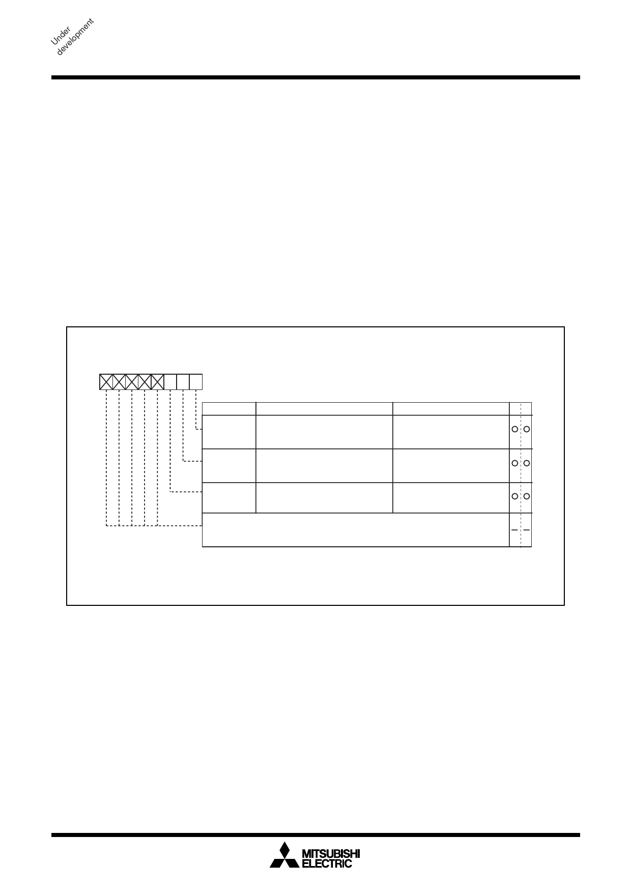
Protect register
b7 b6 b5 b4 b3 b2 b1 b0
Symbol
PRCR
Address When reset
000A16 XXXXX0002
Bit symbol
Bit name
Function
PRC0
Enables writing to system clock
control registers 0 and 1 (addresses 0 : Write-inhibited
000616 and 000716)
1 : Write-enabled
PRC1
Enables writing to processor mode
registers 0 and 1 (addresses 000416
and 000516)
0 : Write-inhibited
1 : Write-enabled
PRC2
Enables writing to port P4 direction 0 : Write-inhibited
register (address 03EA16) (Note)
1 : Write-enabled
RW
Nothing is assigned.
These bits can neither be set nor reset. When read, their contents are
indeterminate.
Note: Writing a value to an address after “1” is written to this bit returns the bit
to “0” . Other bits do not automatically return to “0” and they must therefore
be reset by the program.
Figure 1.21. Protect register
27
Share Link: 