74173 View Datasheet(PDF) - Philips Electronics
Part Name
Description
MFG CO.
74173 Datasheet PDF : 10 Pages
| |||
Philips Semiconductors
Quad D-type flip-flop; positive-edge trigger;
3-state
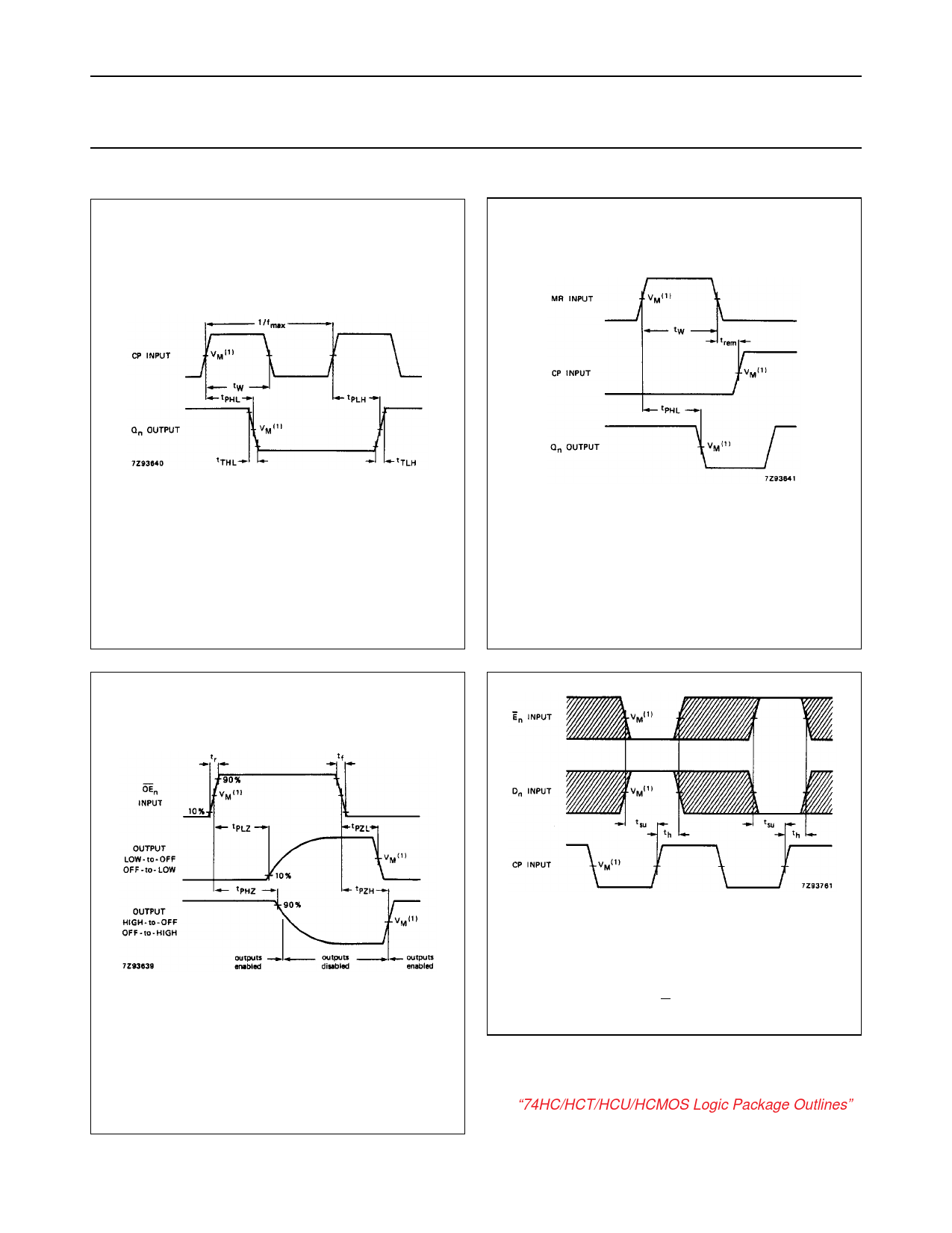
AC WAVEFORMS
Product specification
74HC/HCT173
(1) HC : VM = 50%; VI = GND to VCC.
HCT: VM = 1.3 V; VI = GND to 3 V.
Fig.6
Waveforms showing the clock (CP) to
output (Qn) propagation delays, the clock
pulse width, the output transition times and
the maximum clock pulse frequency.
(1) HC : VM = 50%; VI = GND to VCC.
HCT: VM = 1.3 V; VI = GND to 3 V.
Fig.7
Waveforms showing the master reset (MR)
pulse width, the master reset to output (Qn)
propagation delays and the master reset to
clock (CP) removal time.
(1) HC : VM = 50%; VI = GND to VCC.
HCT: VM = 1.3 V; VI = GND to 3 V.
Fig.8 Waveforms showing the 3-state enable and
disable times.
The shaded areas indicate when the input is permitted to
change for predictable output performance.
(1) HC : VM = 50%; VI = GND to VCC.
HCT: VM = 1.3 V; VI = GND to 3 V.
Fig.9 Waveforms showing the data set-up and hold
times from input (En, Dn) to clock (CP).
PACKAGE OUTLINES
See “74HC/HCT/HCU/HCMOS Logic Package Outlines”.
December 1990
10
Share Link: 