MM74HC165M View Datasheet(PDF) - Fairchild Semiconductor
Part Name
Description
MFG CO.
MM74HC165M Datasheet PDF : 8 Pages
| |||
September 1983
Revised February 1999
MM74HC165
Parallel-in/Serial-out 8-Bit Shift Register
General Description
The MM74HC165 high speed PARALLEL-IN/SERIAL-OUT
SHIFT REGISTER utilizes advanced silicon-gate CMOS
technology. It has the low power consumption and high
noise immunity of standard CMOS integrated circuits,
along with the ability to drive 10 LS-TTL loads.
This 8-bit serial shift register shifts data from QA to QH
when clocked. Parallel inputs to each stage are enabled by
a low level at the SHIFT/LOAD input. Also included is a
gated CLOCK input and a complementary output from the
eighth bit.
Clocking is accomplished through a 2-input NOR gate per-
mitting one input to be used as a CLOCK INHIBIT function.
Holding either of the CLOCK inputs high inhibits clocking,
and holding either CLOCK input low with the SHIFT/LOAD
input high enables the other CLOCK input. Data transfer
occurs on the positive going edge of the clock. Parallel
loading is inhibited as long as the SHIFT/LOAD input is
HIGH. When taken LOW, data at the parallel inputs is
loaded directly into the register independent of the state of
the clock.
The 74HC logic family is functionally as well as pin-out
compatible with the standard 74LS logic family. All inputs
are protected from damage due to static discharge by inter-
nal diode clamps to VCC and ground.
Features
s Typical propagation delay: 20 ns (clock to Q)
s Wide operating supply voltage range: 2–6V
s Low input current: 1 µA maximum
s Low quiescent supply current: 80 µA maximum (74HC
Series)
s Fanout of 10 LS-TTL loads
Ordering Code:
Order Number Package Number
Package Description
MM74HC165M
M16A
16-Lead Small Outline Integrated Circuit (SOIC), JEDEC MS-012, 0.150” Narrow
MM74HC165SJ
M16D
16-Lead Small Outline Package (SOP), EIAJ TYPE II, 5.3mm Wide
MM74HC165MTC
MTC16
16-Lead Thin Shrink Small Outline Package (TSSOP), JEDEC MO-153, 4.4mm Wide
MM74HC165
N16E
16-Lead Plastic Dual-In-Line Package (PDIP), JEDEC MS-001, 0.300” Wide
Devices also available in Tape and Reel. Specify by appending the suffix letter “X” to the ordering code.
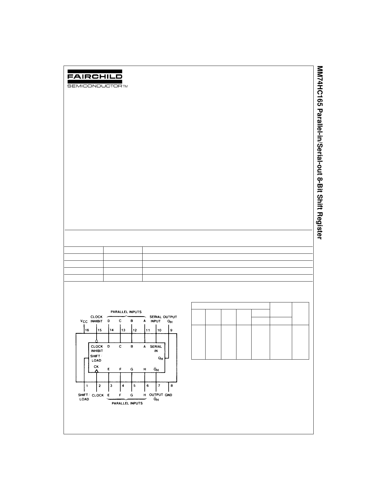
Connection Diagram
Function Table
Pin Assignments for DIP, SOIC, SOP and TSSOP
Inputs
Internal Output
Shift/ Clock Clock Serial Parallel Outputs QH
Load Inhibit
A. . .H QA QB
L
X
X
X a. . .h a b
h
H
L
L
X
X QA0 QB0 QH0
H
L
↑
H
X
H QAN QGN
H
L
↑
L
X
L QAN QGN
H
H
X
X
X QA0 QB0 QH0
H = HIGH Level (steady state), L = LOW Level (steady state)
X = Irrelevant (any input, including transitions)
↑ = Transition from LOW-to-HIGH level
QA0, QB0, QH0 = The level of QA, QB, or QH, respectively, before the indi-
cated steady-state input conditions were established.
QAN, QGN = The level of QA or QG before the most recent ↑ transition of the
clock; indicates a one-bit shift.
Top View
© 1999 Fairchild Semiconductor Corporation DS005316.prf
www.fairchildsemi.com
Share Link: 