VP503 View Datasheet(PDF) - SANYO -> Panasonic
Part Name
Description
View to exact match
VP503 Datasheet PDF : 11 Pages
| |||
VP503
Operating Procedures
1. Setting the operating point
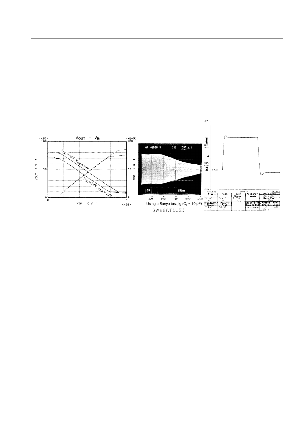
An optimal DC bias must be provided to operate a video pack and acquire the stipulated output dynamic range and
bandwidth characteristics. Basically, the center point output voltage with no input should be set according to the
following formula.
V0 (CENTER) = (VCC + VBB)/2
While the optimal operating point when an AC input is applied will be similar, the recommended electrical
characteristics should be referred to when setting the operating point. The figures below show the DC and AC
waveforms when the Sanyo test jig is used. The design of this product series was optimized so that these products
provide adequate high-power characteristics.
2. Optimal peaking technique for mounted products (VP503 Series)
• Termination LC peaking
As can be seen from the internal equivalent circuit diagram, this series differs from earlier series in that peaking is
not applied using an internal coil. Since the high-frequency region peaking point is determined by an LC resonator
at the termination, the total distributed capacitance of the output side is particularly important. Accordingly, since
the independent evaluation board timing characteristics will differ from the actual output load capacitance when an
output cable is installed, the high-frequency area peaking point that corresponds to the output load state in the
mounted circuit must be found.
(Adjust the circuit using an output matching RC circuit at the same time.)
• RC emitter peaking
The purpose of the emitter peaking value is to increase the AC gain from the mid-frequency area to the high-
frequency area. This should be determined last, after adjusting the termination peaking and output peaking RC
circuits. (To compensate for high-frequency gain degradation at the IC side.)
• Output matching RC circuit
This circuit is used in conjunction with the peaking compensation in each section to match the IC internal
impedance with the output load impedance. Mount this RC circuit in the vicinity of the protection diode and the IC
output pins. Adjust this circuit to correct system characteristics while observing the mid-frequency characteristics,
the amount of overshoot in the pulse response, and other aspects. Since the AC gain from the mid-frequency area to
the high-frequency area will be reduced somewhat by this adjustment, determine the setting by adjusting the value
of the resistor precisely.
The required circuit operating conditions can be set up smoothly if the following flowchart is used to adjust the
peaking values.
No. 4933-5/11
Share Link: 