VP453 View Datasheet(PDF) - SANYO -> Panasonic
Part Name
Description
View to exact match
VP453 Datasheet PDF : 5 Pages
| |||
VP453
Thermal Design
Thermal design requires that the two conditions Tj (max) ≤ 150°C and Tc ≤ 100°C be met.
(a) Concerning Tj (max), the chip temperature Tj for each transistor is given by equation (1).
Tj = (Tri) = θj–c (Tri) × PC (Tri) + ∆Tc + Ta (°C) ................................................(1)
θj–c (Tri): The thermal resistance of each transistor chip itself
PC (Tri): The collector loss for each transistor
∆Tc: Increase in the case temperature
Ta: Ambient temperature
θj–c (Tri) for each chip will be:
θj–c (Tr1) to (Tr4) = 35°C/W ................................................................................(2)
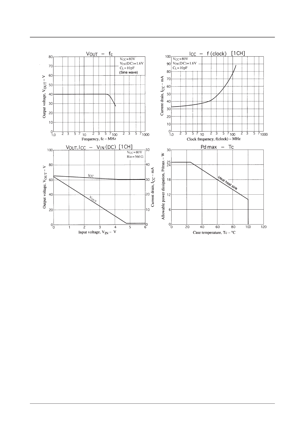
The loss in transistors in a video pack varies with frequency. The loss increases with the frequency.
For example, if the maximum frequency will be 120 MHz (clock), then the transistors with the largest losses will be
transistors 3 and 4 in the emitter-follower (EF) stage. From the Pd – f (clock) figure, we see that that loss will be 25%
of the total for a single channel. That is:
PC (EF stage) f = 120 MHz = Pd (1ch) f = 120 MHz × 0.25 [W]..................................(3)
The thermal design must assure that Tj does not exceed 150°C at this time.
(b) Concerning Tc(max), the relationship between θh and ∆Tc is:
∆Tc = Pd (total) × θh .............................................................................................(4)
Taking the increase due to Ta into account, the condition the thermal design must meet becomes Tc = ∆Tc + Ta <
100°C.
Next we design thermal conditions for the VP453 that meet the conditions in sections (a) and (b) above.
No. 5477-3/5
Share Link: 