CY7C1041BNV33L-12ZXC(2011) View Datasheet(PDF) - Cypress Semiconductor
Part Name
Description
View to exact match
CY7C1041BNV33L-12ZXC Datasheet PDF : 14 Pages
| |||
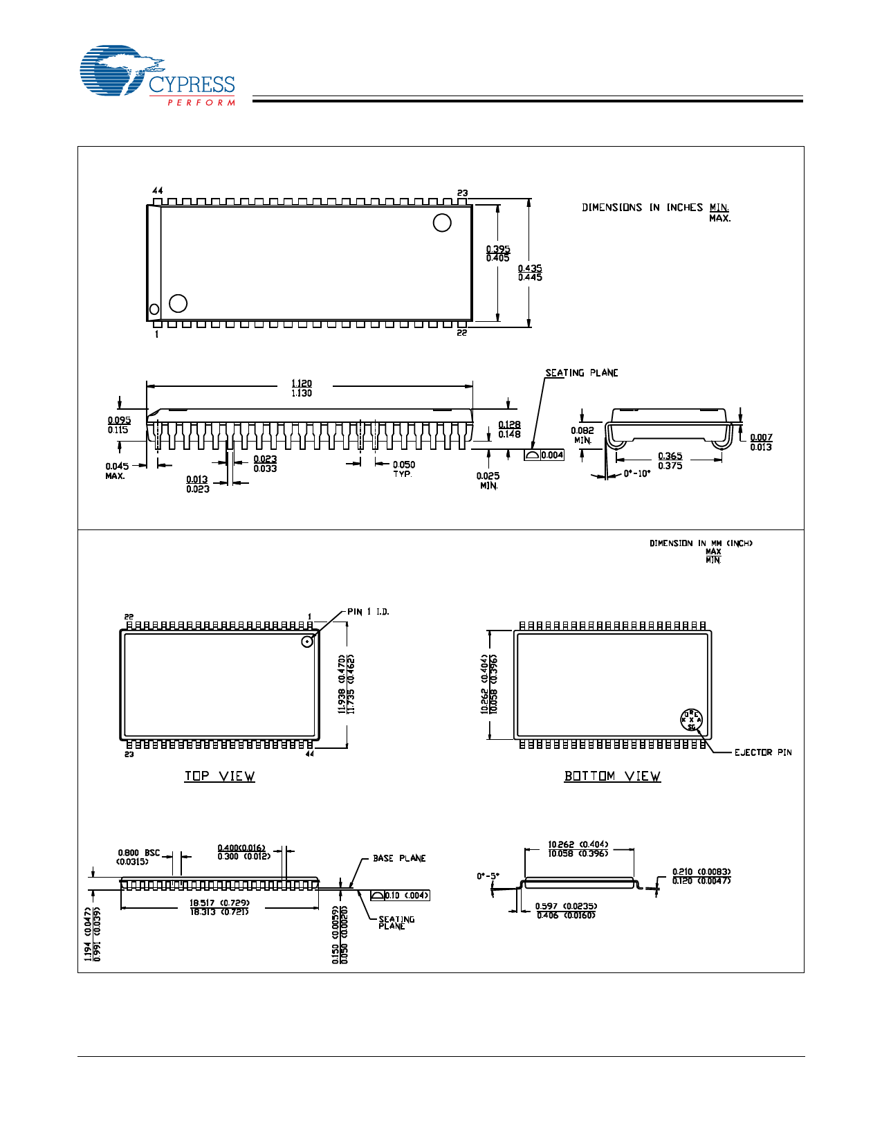
CY7C1041BNV33
Switching Waveforms
Read Cycle No. 1[12, 13]
tRC
ADDRESS
DATA OUT
tAA
tOHA
PREVIOUS DATA VALID
Read Cycle No. 2 (OE Controlled)[13, 14]
DATA VALID
ADDRESS
CE
OE
BHE, BLE
DATA OUT
VCC
SUPPLY
CURRENT
tRC
tACE
tDOE
tLZOE
tDBE
tLZBE
HIGH IMPEDANCE
tLZCE
tPU
50%
DATA VALID
tHZOE
tHZCE
tHZBE
HIGH
IMPEDANCE
tPD
ICC
50%
ISB
Notes
12. Device is continuously selected. OE, CE, BHE and/or BHE = VIL.
13. WE is HIGH for read cycle.
14. Address valid prior to or coincident with CE transition LOW.
Document #: 001-06434 Rev. *C
Page 7 of 14
[+] Feedback
Share Link: 