AT27BV040 View Datasheet(PDF) - Atmel Corporation
Part Name
Description
View to exact match
AT27BV040 Datasheet PDF : 12 Pages
| |||

Features
• Fast Read Access Time - 120 ns
• Dual Voltage Range Operation
– Unregulated Battery Power Supply Range, 2.7V to 3.6V
or Standard 5V ± 10% Supply Range
• Compatible with JEDEC Standard AT27C040
• Low Power CMOS Operation
– 20 µA max. (less than 1 µA typical) Standby for VCC = 3.6V
– 36 mW max. Active at 5 MHz for VCC = 3.6V
• JEDEC Standard Packages
– 32-Lead PLCC
– 32-Lead TSOP (8 x 20 mm)
– 32-Lead VSOP (8 x 14 mm)
• High Reliability CMOS Technology
– 2,000V ESD Protection
– 200 mA Latchup Immunity
• Rapid™ Programming Algorithm - 100 µs/byte (typical)
• CMOS and TTL Compatible Inputs and Outputs
– JEDEC Standard for LVTTL and LVBO
• Integrated Product Identification Code
• Commercial and Industrial Temperature Ranges
Description
The AT27BV040 chip is a high performance, low power, low voltage, 4,194,304-bit
one-time programmable read only memory (EPROM) organized as 512K by 8 bits. It
requires only one supply in the range of 2.7 to 3.6V in normal read mode operation,
making it ideal for fast, portable systems using either regulated or unregulated battery
power.
(continued)
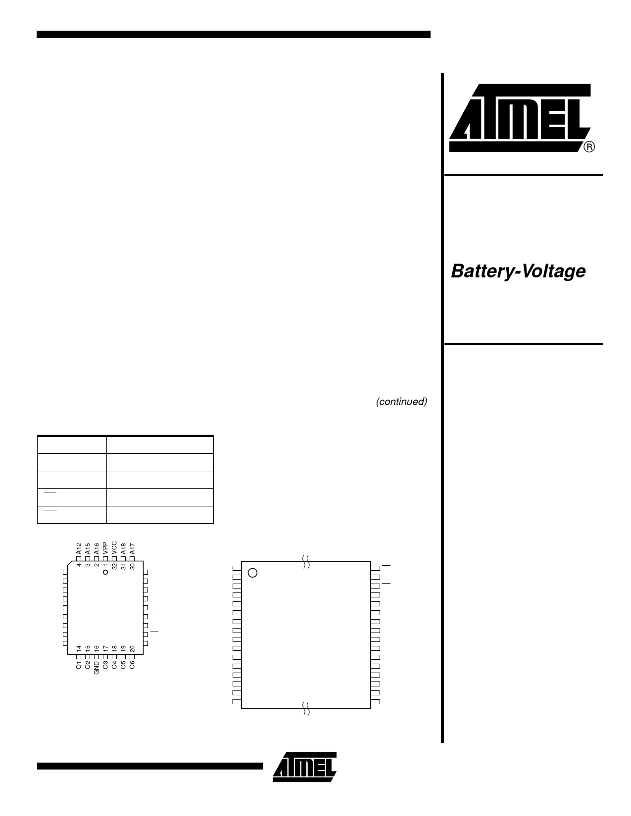
Pin Configurations
Pin Name
Function
A0 - A18
Addresses
O0 - O7
Outputs
CE
Chip Enable
OE
Output Enable
PLCC Top View
TSOP, VSOP Top View
Type 1
A7 5
A6 6
A5 7
A4 8
A3 9
A2 10
A1 11
A0 12
O0 13
29 A14
28 A13
27 A8
26 A9
25 A11
24 OE
23 A10
22 CE
21 O7
A11 1
A9 2
A8 3
A13 4
A14 5
A17 6
A18 7
VCC 8
VPP 9
A16 10
A15 11
A12 12
A7 13
A6 14
A5 15
A4 16
32 OE
31 A10
30 CE
29 O7
28 O6
27 O5
26 O4
25 O3
24 GND
23 O2
22 O1
21 O0
20 A0
19 A1
18 A2
17 A3
4-Megabit
(512K x 8)
Unregulated
Battery-Voltage™
High-Speed OTP
EPROM
AT27BV040
Rev. 0346D–10/98
1