AT27BV040(2007) View Datasheet(PDF) - Atmel Corporation
Part Name
Description
View to exact match
AT27BV040
(Rev.:2007)
(Rev.:2007)
Atmel Corporation

AT27BV040 Datasheet PDF : 15 Pages
| |||
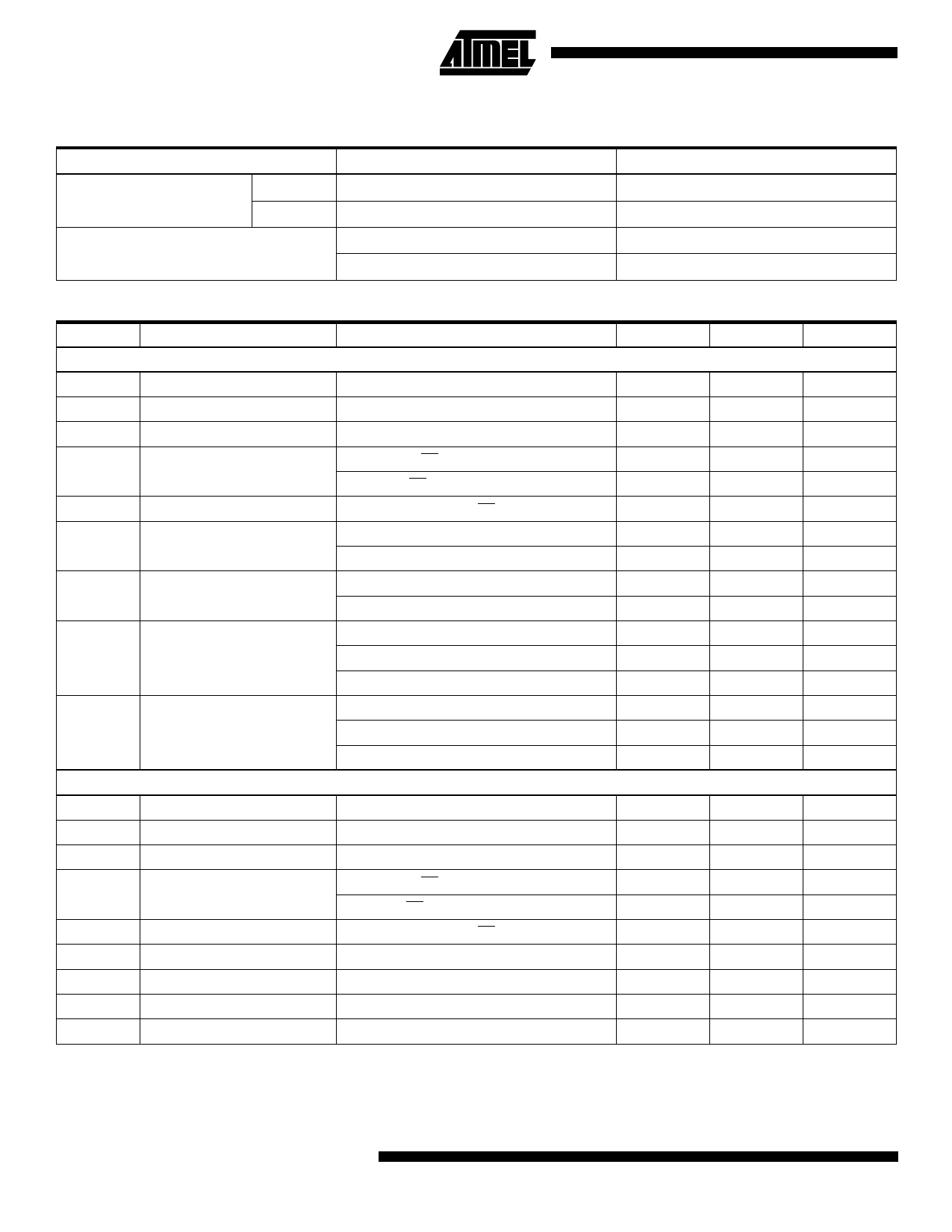
6. Operating Modes
Mode/Pin
CE
OE
Ai
VPP
VCC
Outputs
Read(2)
VIL
VIL
Ai
X(1)
VCC(2)
DOUT
Output Disable(2)
X
VIH
X
X
VCC(2)
High Z
Standby(2)
VIH
X
X
X
VCC(2)
High Z
Rapid Program(3)
VIL
VIH
Ai
VPP
VCC(3)
DIN
PGM Verify(3)
X
VIL
Ai
VPP
VCC(3)
DOUT
PGM Inhibit(3)
VIH
VIH
X
VPP
VCC(3)
High Z
A9 = VH(4)
Product Identification(3)(5)
VIL
VIL
A0 = VIH or VIL
X
A1 - A18 = VIL
VCC(3)
Identification Code
Notes: 1. X can be VIL or VIH.
2. Read, output disable, and standby modes require, 2.7V ≤VCC ≤3.6V, or 4.5V ≤VCC ≤5.5V.
3. Refer to Programming Characteristics. Programming modes require VCC = 6.5V.
4. VH = 12.0 ± 0.5V.
5. Two identifier bytes may be selected. All Ai inputs are held low (VIL), except A9 which is set to VH and A0 which is toggled
low (VIL) to select the Manufacturer’s Identification byte and high (VIH) to select the Device Code byte.
7. DC and AC Operating Conditions for Read Operation
Industrial Operating Temperature (Case)
VCC Power Supply
AT27BV040-12
-40°C - 85°C
2.7V to 3.6V
5V ± 10%
4 AT27BV040
0346G–EPROM–12/07
Share Link: