VP5511C View Datasheet(PDF) - Mitel Networks
Part Name
Description
View to exact match
VP5511C Datasheet PDF : 16 Pages
| |||
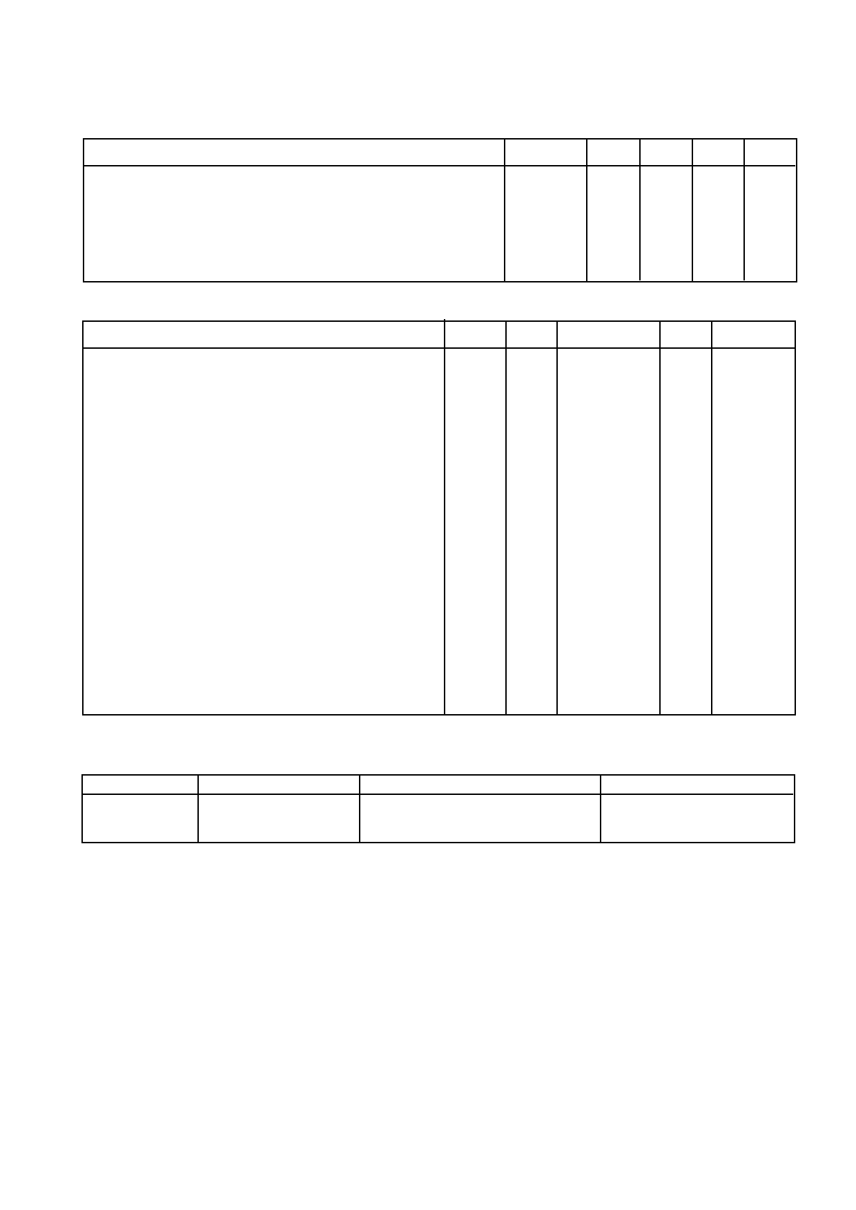
RECOMMENDED OPERATING CONDITIONS
Parameter
Power supply voltage
Power supply current (including analog outputs)
Input clock frequency
SCL clock frequency
Analog video output load
DAC gain resistor
Ambient operating temperature
VIDEO CHARACTERISTICS
Parameter
Luminance bandwidth (high)
Luminance bandwidth (medium)
Luminance bandwidth (low)
Chrominance bandwidth (Extended B/W mode)
Chrominance bandwidth (Reduced B/W mode)
Burst frequency (NTSC)
Burst frequency (PAL-B, D,G,H,I)
Burst frequency (PAL-M)
Burst frequency (PAL-N Argentina)
Burst cycles (NTSC and PAL-M,N)
Burst cycles (PAL-B, D, G, H,I)
Burst envelope rise / fall time (all standards)
Analog video sync rise / fall time (NTSC and PAL-M,N)
Analog video sync rise / fall time (PAL-B, D, G, H,I)
Differential gain
Differential phase
Signal to noise ratio (unmodulated ramp)
Chroma AM signal to noise ratio (100% red field)
Chroma PM signal to noise ratio (100% red field)
Hue accuracy
Colour saturation accuracy
Residual sub carrier
Luminance / chrominance delay
VP5311C/VP5511C
Symbol Min. Typ. Max. Units
VDD, AVDD 4.75
IDD
PXCK -50ppm
fSCL
0
5.00
150
27.00
37.5
769
5.25
+50ppm
500
70
V
mA
MHz
kHz
Ω
Ω
°C
Symbol Min.
-5
Typ.
6.16
4.34
2.79
1.3
650
3.57954545
4.43361875
3.57561189
3.58205625
9
10
300
145
245
1.0
0.5
-60
0
Max.
-61
-56
-58
2.5
2.5
+5
Units
MHz
MHz
MHz
MHz
kHz
MHz
MHz
MHz
MHz
Fsc cycles
Fsc cycles
ns
ns
ns
% pk-pk
° pk-pk
dB
dB
dB
%
%
dB
ns
ESD COMPLIANCE
Pins
All pins
Test
Human body model
All pins
Machine model
Test Levels
2kV on 100pF through 1k5Ω
200V on 200pF through 0Ω & 500nH
Notes
Meets Mil-Std-883 Class 2
3
Share Link: 