PD45128163G5-A10LI-9JF View Datasheet(PDF) - Elpida Memory, Inc
Part Name
Description
View to exact match
PD45128163G5-A10LI-9JF
Elpida Memory, Inc

PD45128163G5-A10LI-9JF Datasheet PDF : 89 Pages
| |||
µPD45128441-I, 45128841-I, 45128163-I
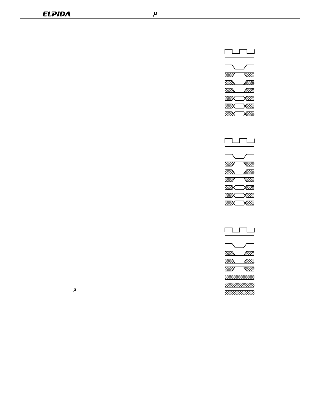
Write command
Fig.4 Column address and write command
(/CS, /CAS, /WE = Low, /RAS = High)
If the mode register is in the burst write mode, this command sets the
burst start address given by the column address to begin the burst
write operation. The first write data in burst mode can input with this
command with subsequent data on following clocks.
CLK
CKE
/CS
/RAS
/CAS
/WE
BA0(A13), BA1(A12)
A10
Add
H
Col.
Read command
Fig.5 Column address and read command
(/CS, /CAS = Low, /RAS, /WE = High)
Read data is available after /CAS latency requirements have been
met. This command sets the burst start address given by the column
address.
CLK
CKE
/CS
/RAS
/CAS
/WE
BA0(A13), BA1(A12)
A10
Add
H
Col.
CBR (auto) refresh command
(/CS, /RAS, /CAS = Low, /WE, CKE = High)
This command is a request to begin the CBR (auto) refresh
operation. The refresh address is generated internally.
Before executing CBR (auto) refresh, all banks must be precharged.
After this cycle, all banks will be in the idle (precharged) state and
ready for a row activate command.
During tRC period (from refresh command to refresh or activate
command), the µPD45128xxx cannot accept any other command.
Fig.6 CBR (auto) refresh command
CLK
CKE H
/CS
/RAS
/CAS
/WE
BA0(A13), BA1(A12)
A10
Add
12
Preliminary Data Sheet E0233N10
Share Link: