ISL8014 View Datasheet(PDF) - Renesas Electronics
Part Name
Description
View to exact match
ISL8014 Datasheet PDF : 17 Pages
| |||
ISL8014
Absolute Maximum Ratings (Reference to GND)
VIN, VDD . . . . . . . . . . . . . . -0.3V to 6V (DC) or 7V (20ms)
EN, SYNCH, PG . . . . . . . . . . . . . . . . . . -0.3V to VIN + 0.3V
LX . . . -1.5V (100ns)/-0.3V (DC) to 6.5V (DC) or 7V (20ms)
VFB . . . . . . . . . . . . . . . . . . . . . . . . . . . . . . -0.3V to 2.7V
Recommended Operating Conditions
VIN Supply Voltage Range . . . . . . . . . . . . . . . . 2.7V to 5.5V
Load Current Range . . . . . . . . . . . . . . . . . . . . . . . 0A to 4A
Ambient Temperature Range . . . . . . . . . . . . -40°C to +85°C
Thermal Information
Thermal Resistance (Typical, Notes 4, 5)JA (°C/W)JC (°C/W)
16 Ld 4x4 QFN Package . . . . . . .
39
3
Junction Temperature Range . . . . . . . . . . -55°C to +125°C
Storage Temperature Range . . . . . . . . . . . -65°C to +150°C
Pb-Free Reflow Profile . . . . . . . . . . . . . . . . . .see link below
http://www.intersil.com/pbfree/Pb-FreeReflow.asp
CAUTION: Do not operate at or near the maximum ratings listed for extended periods of time. Exposure to such conditions may adversely impact
product reliability and result in failures not covered by warranty.
NOTE:
4. JA is measured in free air with the component mounted on a high effective thermal conductivity test board with “direct attach”
features. See Tech Brief TB379.
5. JC, “case temperature” location is at the center of the exposed metal pad on the package underside. See Tech Brief TB379.
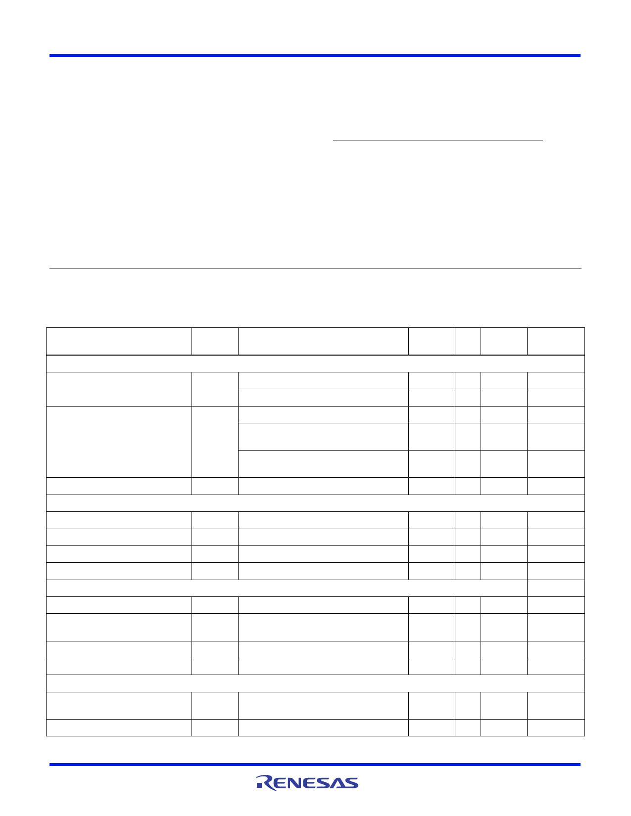
Electrical Specifications
PARAMETER
INPUT SUPPLY
VDD Undervoltage Lockout
Threshold
Quiescent Supply Current
Shut Down Supply Current
OUTPUT REGULATION
Reference Voltage
VFB Bias Current
Line Regulation
Soft-Start Ramp Time Cycle
OVERCURRENT PROTECTION
Current Limit Blanking Time
Overcurrent and Auto Restart
Period
Switch Current Limit
Peak Skip Limit
COMPENSATION
Error Amplifier
Trans-Conductance
Trans-Resistance
Unless otherwise noted, all parameter limits are established over the recommended
operating conditions and the typical specification are measured at the following conditions:
TA = -40°C to +85°C, VIN = 3.6V, EN = VDD, unless otherwise noted. Typical values are at
TA = +25°C. Boldface limits apply over the operating temperature range,
-40°C to +85°C.
SYMBOL
TEST CONDITIONS
MIN
MAX
(Note 7) TYP (Note 7)
UNITS
VUVLO
IVIN
ISD
Rising, no load
Falling, no load
SYNCH = GND, no load at the output
SYNCH = GND, no load at the output
and no switches switching
SYNCH = VDD, FS = 1MHz, no load at
the output
VIN = 5.5V, EN = low
-
2.5
2.7
2.2
2.4
-
-
35
-
-
30
45
-
6.5
10
-
0.1
2
VREF
0.790 0.8 0.810
IVFB VFB = 0.75V
-
0.1
-
VIN = VO + 0.5V to 5.5V (minimal 2.7V)
-
0.2
-
-
1
-
V
V
µA
µA
mA
µA
V
µA
%/V
ms
tOCON
tOCOFF
ILIMIT
ISKIP
(Note 6)
(Note 6)
RT
-
17
-
Clock pulses
-
4
-
SS cycle
4.9
6.0
7.1
A
-
1.3
-
A
-
20
-
0.17 0.20 0.23
µA/V
FN6576 Rev 4.00
November 23, 2009
Page 4 of 17
Share Link: 