VP5513 View Datasheet(PDF) - Zarlink Semiconductor Inc
Part Name
Description
View to exact match
VP5513 Datasheet PDF : 19 Pages
| |||
VP5313/VP5513
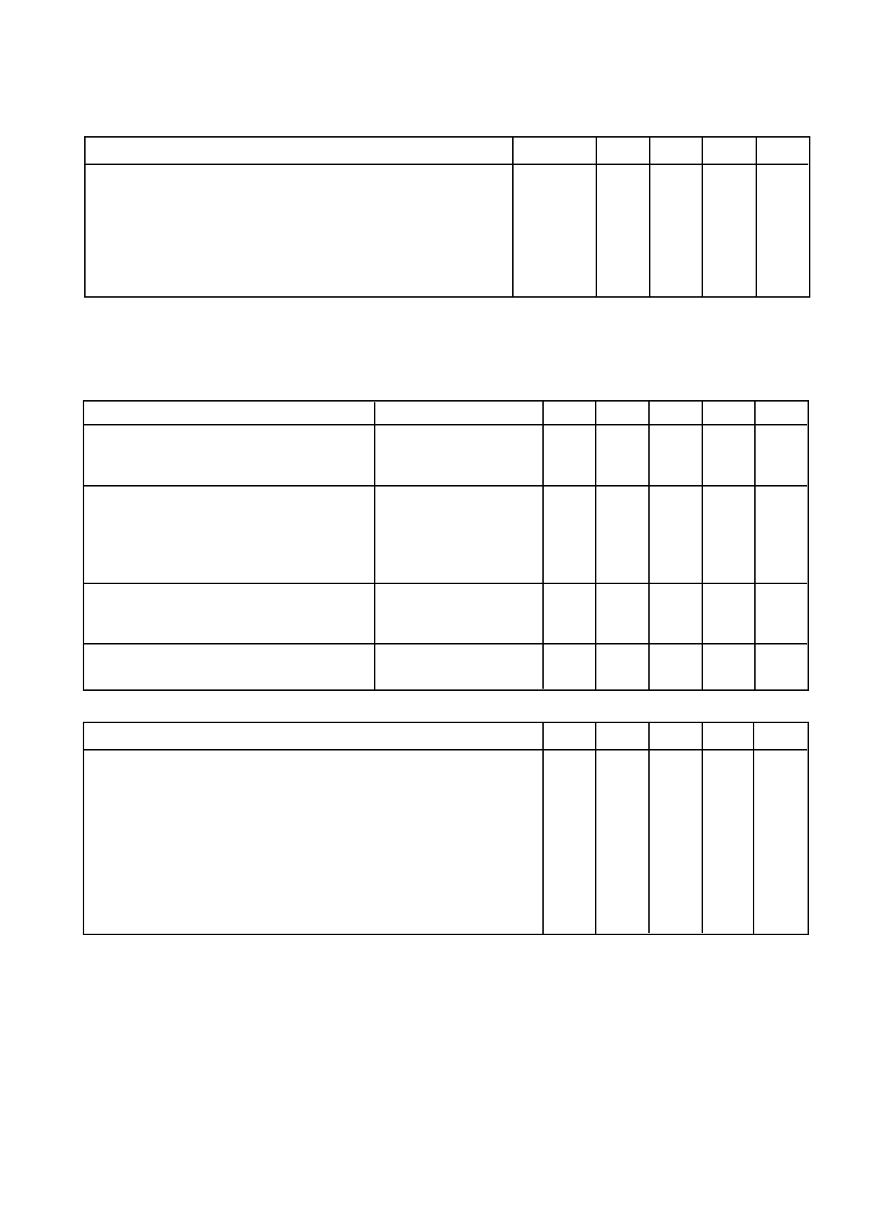
RECOMMENDED OPERATING CONDITIONS
Parameter
Power supply voltage
Power supply current (including analog outputs)1
Power supply current (including analog outputs)2
Input clock frequency
SCL clock frequency
Analog video output load
DAC gain resistor
Ambient operating temperature
1. All four DACs driving 37R5 loads
2. All four DACs driving 75R loads
Symbol Min. Typ. Max. Units
VDD, AVDD 4.75
IDD
IDD
PXCK -50ppm
fSCL
0
5.00
27.00
37.5
730
5.25
230
190
+50ppm
500
70
V
mA
mA
MHz
kHz
Ω
Ω
°C
ELECTRICAL CHARACTERISTICS
Test conditions (unless otherwise stated): As specified in Recommended Operating Conditions
DC CHARACTERISTICS
Parameter
Conditions
Symbol Min. Typ. Max. Units
Digital Inputs TTL compatible (except SDA, SCL)
Input high voltage
Input low voltage
VIN 2.0
VIL
V
0.8
V
Digital Inputs SDA, SCL
Input high voltage
Input low voltage
Input high current
Input low current
VIN = VDD
VIN = VSS
VIH 0.7VDD
VIL
IIH
IIL
V
0.3VDD V
10
µA
-10
µA
Digital Outputs CMOS compatible
Output high voltage
Output low voltage
IOH = -1mA
IOL = +4mA
VOH 3.7
VOL
V
0.4
V
Digital Output SDA
Output low voltage
IOL = +6mA
VOL
0.6
V
DC CHARACTERISTICS DACs
Parameter
Accuracy (each DAC)
Integral linearity error
Diffential linearity error
DAC matching error
Monotonicity
LSB size
Internal reference voltage
Internal reference voltage output impedance
Reference Current (VREF/RREF) RREF = 730Ω
Maximum output
Peak Glitch Energy (see fig.3)
Symbol Min. Typ. Max. Units
INL
DNL
VREF
ZR
IREF
0.95
guaranteed
66.83
1.00
8k
1.3899
34.15
50
±1.5
±1
±5
1.05
LSB
LSB
%
µA
V
Ω
mA
mA
pV-s
ABSOLUTE MAXIMUM RATINGS
Supply voltage
VDD, AVDD
Voltage on any non power pin
Ambient operating temperature
Storage temperature
-0·3 to 7·0V
-0·3 to VDD+0·3V
0 to 70°C
-55°C to 150°C
Note: Stresses exceeding these listed under Absolute
Maximum Ratings may induce failure. Exposure to Absolute
Maximum Ratings for extended periods may reduce
reliability. Functionality at or above these conditions is not
implied.
2
Share Link: 