74ABT648PW,118 View Datasheet(PDF) - NXP Semiconductors.
Part Name
Description
View to exact match
74ABT648PW,118 Datasheet PDF : 19 Pages
| |||
Philips Semiconductors
74ABT648
Octal transceiver/register; inverting; 3-state
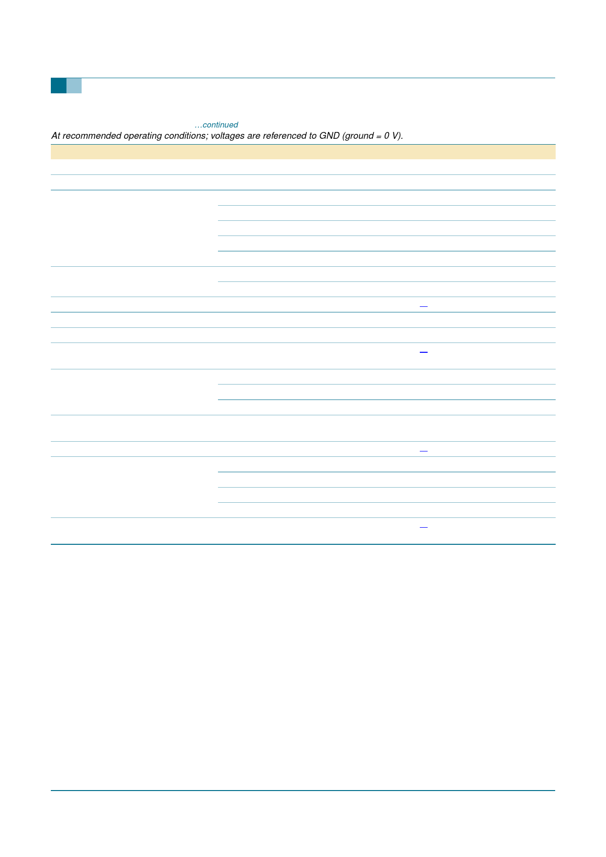
Table 7: Static characteristics …continued
At recommended operating conditions; voltages are referenced to GND (ground = 0 V).
Symbol Parameter
Conditions
Tamb = −40 °C to +85 °C
VIK
input diode voltage
VOH
HIGH-level output voltage
VOL
LOW-level output voltage
VRST
ILI
IOFF
IPU, IPD
IOZ
power-up output low voltage
input leakage current
power-off leakage current
power-up or power-down
down 3-state output current
3-state output current
ICEX
output HIGH-state leakage
current
VCC = 4.5 V; IIK = −18 mA
VCC = 4.5 V; VI = VIL or VIH
IO = −3 mA
IO = −32 mA
VCC = 5.0 V; VI = VIL or VIH
IO = −3 mA
VCC = 4.5 V; VI = VIL or VIH
IO = 64 mA
VCC = 5.5 V; IO = 1 mA; VI = GND or VCC
VCC = 5.5 V; VI = GND or 5.5 V
VCC = 0.0 V; VO or VI ≤ 4.5 V
VCC = 2.1 V; VO = 0.5 V; VI = GND or VCC;
VOE = don’t care
VCC = 5.5 V; VI = VIL or VIH
output HIGH-state at VO = 2.7 V
output LOW-state at VO = 0.5 V
VCC = 5.5 V; VO = 5.5 V; VI = GND or VCC
IO
output current
VCC = 5.5 V; VO = 2.5 V
ICC
quiescent supply current
VCC = 5.5 V; VI = GND or VCC
outputs HIGH-state
outputs LOW-state
outputs 3-state
∆ICC
additional supply current per one data input at 3.4 V and other inputs at
data input pin
VCC or GND; VCC = 5.5 V
Min
-
2.5
2.0
3.0
-
[1] -
-
-
[2] -
-
-
-
[3] −50
-
-
-
[4]
Typ Max Unit
-
−1.2 V
-
-
V
-
-
V
-
-
V
-
0.55 V
-
0.55 V
-
±1.0 µA
-
±100 µA
-
±50 µA
-
50 µA
-
−50 µA
-
50 µA
-
−180 mA
-
250 µA
-
30 mA
-
250 µA
1.5 mA
[1] For valid test results, data must not be loaded into the flip-flops (or latches) after applying the power.
[2] This parameter is valid for any VCC between 0 V and 2.1 V, with a transition time of up to 10 ms. From VCC = 2.1 V to VCC = 5 V ± 10 %
a transition time of up to 100 µs is permitted.
[3] Not more than one output should be tested at a time, and the duration of the test should not exceed one second.
[4] This is the increase in supply current for each input at 3.4 V.
9397 750 14858
Product data sheet
Rev. 04 — 27 April 2005
© Koninklijke Philips Electronics N.V. 2005. All rights reserved.
9 of 19
Share Link: 