BSB012NE2LX View Datasheet(PDF) - Infineon Technologies
Part Name
Description
View to exact match
BSB012NE2LX Datasheet PDF : 13 Pages
| |||
OptiMOS™ Power-MOSFET
BSB012NE2LX
2
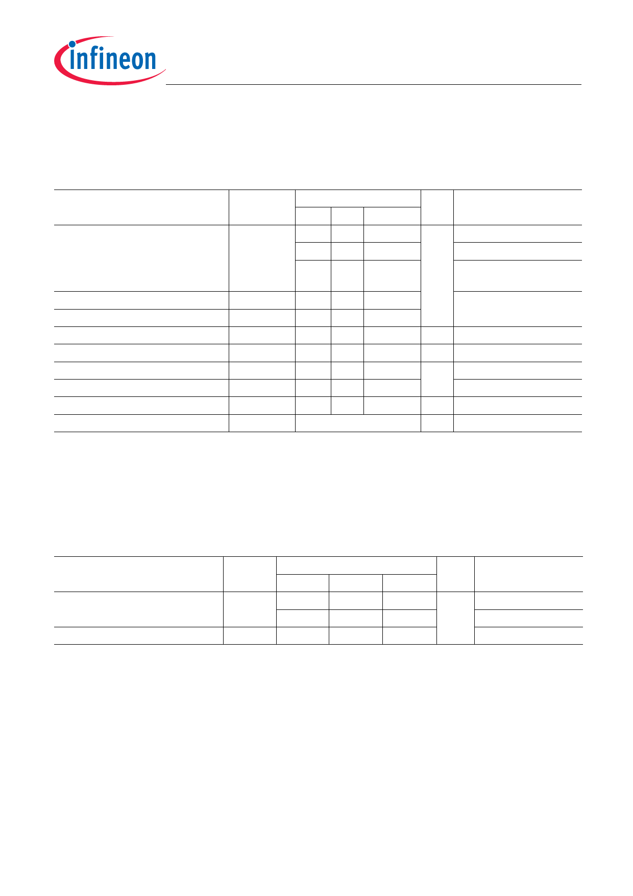
Maximum ratings
at Tj = 25 °C, unless otherwise specified.
Table 2 Maximum ratings
Parameter
Symbol
Continuous drain current
ID
Pulsed drain current1)
Avalanche current, single pulse2)
Avalanche energy, single pulse
Gate source voltage
Power dissipation
ID,pulse
IAS
EAS
VGS
Ptot
Operating and storage temperature Tj,Tstg
IEC climatic category; DIN IEC 68-1
1) See figure 3 for more detailed information
2) See figure 13 for more detailed information
Min.
-
-
-
Values
Typ. Max.
-
170
-
107
-
37
-
-
400
-
-
40
-
-
240
-20 -
20
-
-
57
-
-
2.8
-40 -
150
55/150/56
Unit Note / Test Condition
A
VGS=10 V, TC=25 °C
VGS=10 V, TC=100 °C
VGS=10 V, TA=25 °C,
RthJA=45 K/W)
TC=25 °C
mJ ID=40 A,RGS=25 Ω
V
W TC=25 °C
TA=25 °C, RthJA=45 K/W
°C
3
Thermal characteristics
Table 3 Thermal characteristics
Parameter
Symbol
Min.
Values
Typ.
Max.
Unit Note /
Test Condition
Thermal resistance, junction - case RthJC
-
1.0
-
°K/W bottom
-
-
2.2
top
Device on PCB
RthJA
-
-
45
6 cm2 cooling area1)
1) Device on 40 mm x 40 mm x 1.5 mm epoxy PCB FR4 with 6 cm2 (one layer, 70µ, thick) copper area for drain conneciton.
PCB is vertical in still air.
Final Data Sheet
2
2.0, 2011-03-18
Share Link: 