BSB008NE2LX View Datasheet(PDF) - Infineon Technologies
Part Name
Description
View to exact match
BSB008NE2LX Datasheet PDF : 15 Pages
| |||
OptiMOSTMPower-MOSFET,25V
BSB008NE2LX
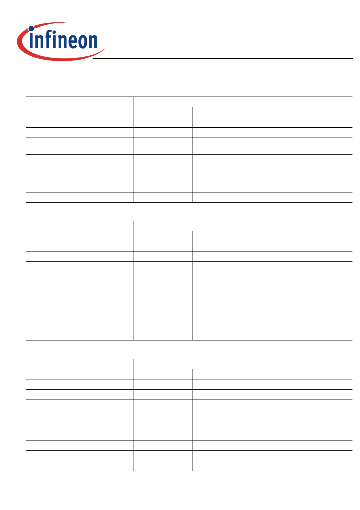
4Electricalcharacteristics
Table4Staticcharacteristics
Parameter
Symbol
Drain-source breakdown voltage
Gate threshold voltage
Zero gate voltage drain current
Gate-source leakage current
Drain-source on-state resistance
Gate resistance
Transconductance
V(BR)DSS
VGS(th)
IDSS
IGSS
RDS(on)
RG
gfs
Min.
25
1.2
-
-
-
-
-
0.3
120
Values
Typ. Max.
-
-
-
2
0.1 10
10 100
10 100
0.75 1.0
0.6 0.8
0.5 1.0
240 -
Unit Note/TestCondition
V VGS=0V,ID=1mA
V
VDS=VGS,ID=250µA
µA
VDS=25V,VGS=0V,Tj=25°C
VDS=25V,VGS=0V,Tj=125°C
nA VGS=20V,VDS=0V
mΩ
VGS=4.5V,ID=25A
VGS=10V,ID=30A
Ω-
S
|VDS|>2|ID|RDS(on)max,ID=30A
Table5Dynamiccharacteristics
Parameter
Symbol
Input capacitance
Ciss
Output capacitance
Coss
Reverse transfer capacitance
Crss
Turn-on delay time
td(on)
Rise time
tr
Turn-off delay time
td(off)
Fall time
tf
Min.
-
-
-
-
-
-
-
Values
Unit Note/TestCondition
Typ. Max.
12000 16000 pF VGS=0V,VDS=12V,f=1MHz
3800 5100 pF VGS=0V,VDS=12V,f=1MHz
3300 -
pF VGS=0V,VDS=12V,f=1MHz
12.6 -
ns
VDD=12V,VGS=10V,ID=30A,
RG,ext=1.6Ω
47.2 -
ns
VDD=12V,VGS=10V,ID=30A,
RG,ext=1.6Ω
75 -
ns
VDD=12V,VGS=10V,ID=30A,
RG,ext=1.6Ω
32.4 -
ns
VDD=12V,VGS=10V,ID=30A,
RG,ext=1.6Ω
Table6Gatechargecharacteristics1)
Parameter
Symbol
Gate to source charge
Gate charge at threshold
Gate to drain charge
Switching charge
Gate charge total
Gate plateau voltage
Gate charge total
Gate charge total, sync. FET
Output charge
Qgs
Qg(th)
Qgd
Qsw
Qg
Vplateau
Qg
Qg(sync)
Qoss
Min.
-
-
-
-
-
-
-
-
-
Values
Typ. Max.
27 36
19 -
73 110
81 -
146 194
2.2 -
258 343
88 -
74 98
Unit Note/TestCondition
nC VDD=12V,ID=30A,VGS=0to4.5V
nC VDD=12V,ID=30A,VGS=0to4.5V
nC VDD=12V,ID=30A,VGS=0to4.5V
nC VDD=12V,ID=30A,VGS=0to4.5V
nC VDD=12V,ID=30A,VGS=0to4.5V
V VDD=12V,ID=30A,VGS=0to4.5V
nC VDD=12V,ID=30A,VGS=0to10V
nC VDS=0.1V,VGS=0to4.5V
nC VDD=12V,VGS=0V
1) See ″Gate charge waveforms″ for parameter definition
Final Data Sheet
5
Rev.2.0,2015-01-20
Share Link: 