74LVC32A View Datasheet(PDF) - NXP Semiconductors.
Part Name
Description
View to exact match
74LVC32A Datasheet PDF : 14 Pages
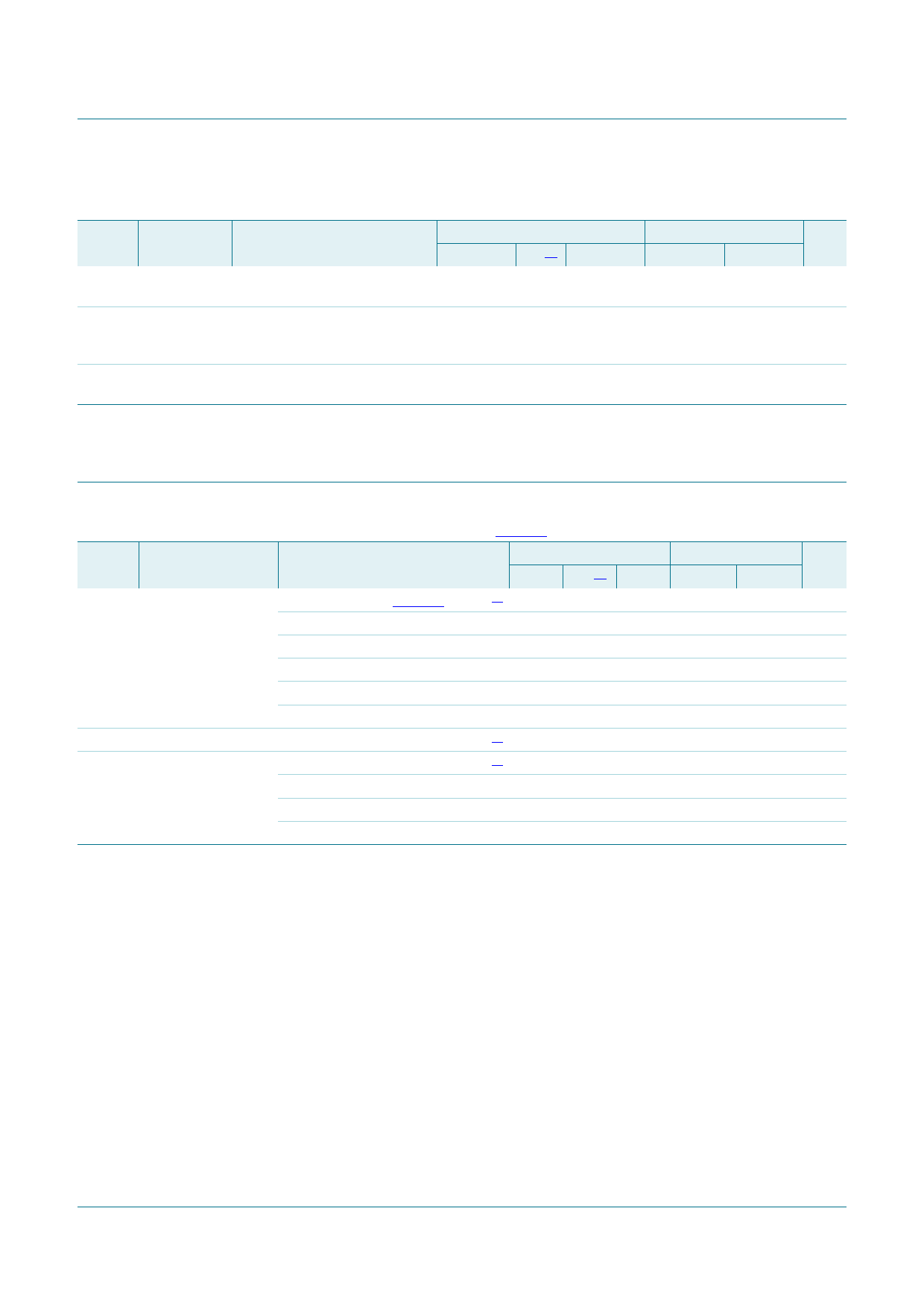
| |||
NXP Semiconductors
74LVC32A
Quad 2-input OR gate
Table 6. Static characteristics …continued
At recommended operating conditions. Voltages are referenced to GND (ground = 0 V).
Symbol Parameter Conditions
40 C to +85 C
Min
Typ[1]
Max
ICC
ICC
supply
current
additional
supply
current
VCC = 3.6 V; VI = VCC or GND; -
IO = 0 A
per input pin;
-
VCC = 2.7 V to 3.6 V;
VI = VCC 0.6 V; IO = 0 A
0.1 10
5
500
CI
input
VCC = 0 V to 3.6 V;
capacitance VI = GND to VCC
-
4.0 -
[1] All typical values are measured at VCC = 3.3 V (unless stated otherwise) and Tamb = 25 C.
10. Dynamic characteristics
40 C to +125 C Unit
Min
Max
-
40
A
-
5 000
A
-
-
pF
Table 7. Dynamic characteristics
Voltages are referenced to GND (ground = 0 V). For test circuit see Figure 7.
Symbol Parameter
Conditions
40 C to +85 C
Min Typ[1] Max
tpd
propagation delay nA, nB to nY; see Figure 6
[2]
VCC = 1.2 V
-
10
-
VCC = 1.65 V to 1.95 V
0.5 4.2 9.0
VCC = 2.3 V to 2.7 V
1.5 2.4 4.9
VCC = 2.7 V
1.5 2.5 4.4
tsk(o)
CPD
output skew time
power dissipation
capacitance
VCC = 3.0 V to 3.6 V
VCC = 3.0 V to 3.6 V
per gate; VI = GND to VCC
VCC = 1.65 V to 1.95 V
1.0 2.2 3.8
[3]
-
-
1.0
[4]
-
4.7
-
VCC = 2.3 V to 2.7 V
-
8.0
-
VCC = 3.0 V to 3.6 V
-
11.0
-
40 C to +125 C Unit
Min
Max
-
- ns
0.5
10.4 ns
1.05
5.7 ns
1.5
5.5 ns
1.0
5.0 ns
-
1.5 ns
-
- pF
-
- pF
-
- pF
[1] Typical values are measured at Tamb = 25 C and VCC = 1.2 V, 1.8 V, 2.5 V, 2.7 V, and 3.3 V respectively.
[2] tpd is the same as tPLH and tPHL.
[3] Skew between any two outputs of the same package switching in the same direction. This parameter is guaranteed by design.
[4] CPD is used to determine the dynamic power dissipation (PD in W).
PD = CPD VCC2 fi N + (CL VCC2 fo) where:
fi = input frequency in MHz; fo = output frequency in MHz
CL = output load capacitance in pF
VCC = supply voltage in Volts
N = number of inputs switching
(CL VCC2 fo) = sum of the outputs
74LVC32A
Product data sheet
All information provided in this document is subject to legal disclaimers.
Rev. 5 — 17 November 2011
© NXP B.V. 2011. All rights reserved.
5 of 14
Share Link: 