CS5210-1GT3 View Datasheet(PDF) - Cherry semiconductor
Part Name
Description
View to exact match
CS5210-1GT3 Datasheet PDF : 8 Pages
| |||
Application Notes: continued
Theory of Operation
The CS5210-1 linear regulator has a composite PNP-NPN
output stage that requires an output capacitor for stability.
A detailed procedure for selecting this capacitor is includ-
ed in the Stability Considerations section.
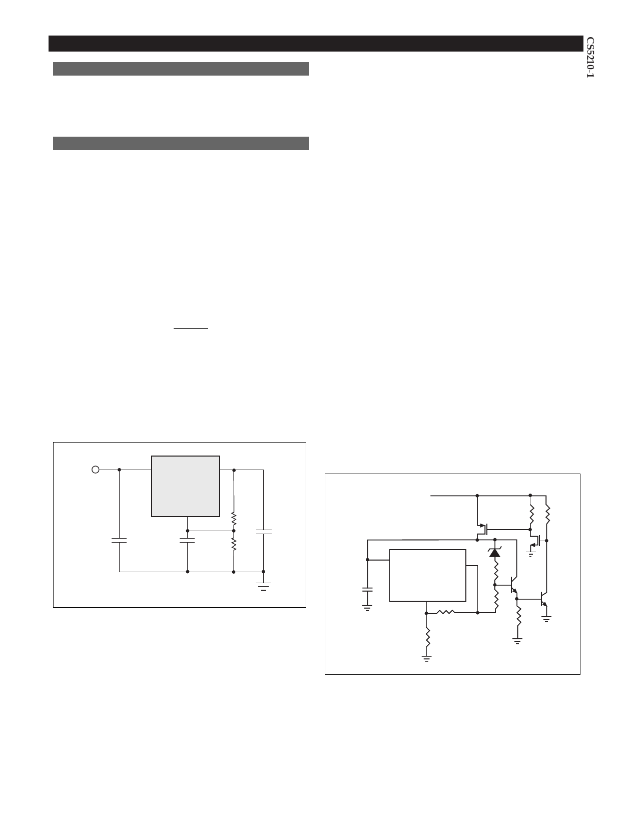
Adjustable Operation
Design Guidelines
This LDO adjustable regulator has an output voltage range
of 1.25V to 4.5V. An external resistor divider sets the out-
put voltage as shown in Figure 1. The regulatorÕs voltage
sensing error amplifier maintains a fixed 1.25V reference
between the output pin and the adjust pin.
A resistor divider network R1 and R2 causes a fixed current
to flow to ground. This current creates a voltage across R2
that adds to the 1.25V across R1 and sets the overall output
voltage. The adjust pin current (typically 50µA) also flows
through R2 and adds a small error that should be taken
into account if precise adjustment of VOUT is necessary.
The output voltage is set according to the formula:
VOUT = VREF ´
R1 + R2
R1
+ R2 ´ IAdj
The term IAdj ´ R2 represents the error added by the adjust
pin current.
R1 is chosen so that the minimum load current is a least
10mA. R1 and R2 should be of the same composition for
best tracking over temperature. The divider resistor
should be placed as close to the IC as possible and connect-
ed to the output with a separate metal trace.
VIN
VOUT
specification of 6V for the voltage difference between VIN
and VOUT. However, the IC may be used to regulate volt-
ages in excess of 6V. The main considerations in such a
design are power-up and short circuit capability.
In most applications, ramp-up of the power supply to VIN
is fairly slow, typically on the order of several tens of mil-
liseconds, while the regulator responds in less than one
microsecond. In this case, the linear regulator begins
charging the output capacitor as soon as the VIN to VOUT
differential is large enough that the pass transistor con-
ducts current. VOUT is essentially at ground, and VIN is on
the order of several hundred millivolts, so that the pass
transistor is in dropout. As VIN increases, the pass transis-
tor will remain in dropout, and current is passed to the
load until VOUT is in regulation. Further increase in VIN
brings the pass transistor out of dropout. The result is that
the output voltage follows the power supply ramp-up,
staying in dropout until the regulation point is reached. In
this manner, any output voltage may be regulated. There
is no theoretical limit to the regulated voltage as long as
the VIN to VOUT differential of 6V is not exceeded.
However, maximum ratings of the IC will be exceeded in a
short circuit condition. Short circuit conditions will result
in the immediate operation of the pass transistor outside of
its safe operating area. Over-voltage stresses will then
cause destruction of the pass transistor before overcurrent
or thermal shutdown circuitry can become active.
Additional circuitry may be required to clamp VIN to VOUT
differential to less than 6V if failsafe operation is required.
One possible clamp circuit is illustrated below; however,
the design of clamp circuitry must be done on an applica-
tion by application basis. Care must be taken to ensure the
clamp actually protects the design. Components used in
the clamp design must be able to withstand the short cir-
cuit conditions indefinitely while protecting the IC.
CS5210-1
Adj
R1
EXTERNAL SUPPLY
R2
Figure 1:
While not required, a bypass capacitor connected between
the adjust pin and ground will improve transient response
and ripple rejection. A 0.1µF tantalum capacitor is recom-
mended for Òfirst cutÓ design. Value and type may be var-
ied to optimize performance vs price.
The CS5210-1 linear regulator has an absolute maximum
Figure 2:
VIN
VOUT
VAdj
5
Share Link: 