LC8220 View Datasheet(PDF) - SANYO -> Panasonic
Part Name
Description
View to exact match
LC8220 Datasheet PDF : 13 Pages
| |||
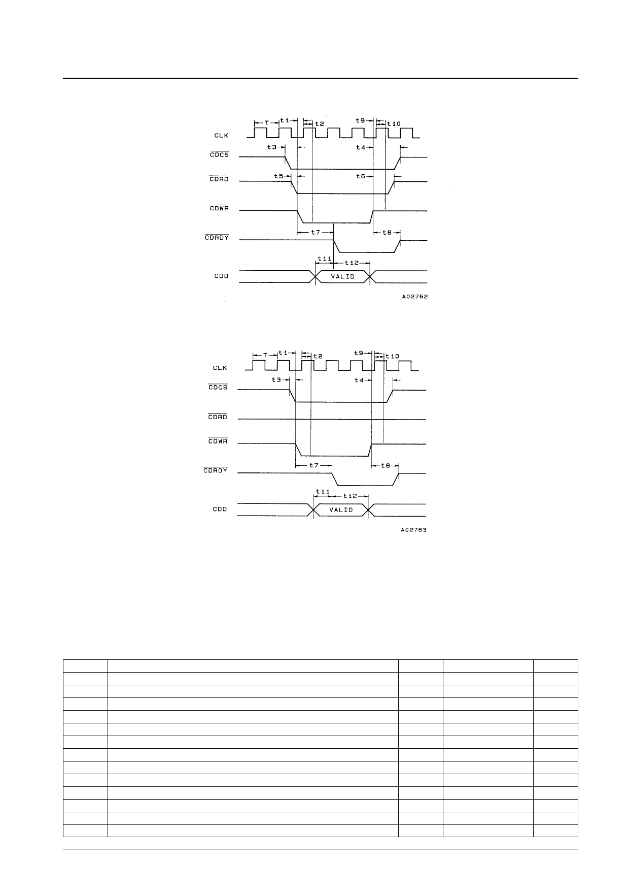
Code Bus Write Cycle
LC8220
Code Bus Write Cycle (type 1)
Code Bus Write Cycle (type 2)
Item
t1
Write signal assert setup time (referenced to CLK)
t2
Write signal assert hold time (referenced to CLK)
t3
Chip select stabilization time (referenced to the write signal)
t4
Chip select hold time (referenced to the write signal)
t5
Write cycle selection signal stabilization time (referenced to the write signal)
t6
Write cycle selection signal hold time (referenced to the write signal)
t7
Ready signal response delay time (referenced to the write signal)
t8
Ready signal release delay time (referenced to the write signal)
t9
Write signal negate setup time (referenced to CLK)
t10
Write signal negate hold time (referenced to CLK)
t11
Data setup time (referenced to the ready signal)
t12
Data hold time (referenced to the ready signal)
T
Clock period
Minimum
8
15
0
0
0
0
8
15
45
15
60
Maximum
T + t1 + 20
t9 + 27
Unit
ns
ns
ns
ns
ns
ns
ns
ns
ns
ns
ns
ns
ns
No. 4909-8/13
Share Link: 