HEF4520BP,652 View Datasheet(PDF) - NXP Semiconductors.
Part Name
Description
View to exact match
HEF4520BP,652 Datasheet PDF : 14 Pages
| |||
NXP Semiconductors
HEF4520B
Dual binary counter
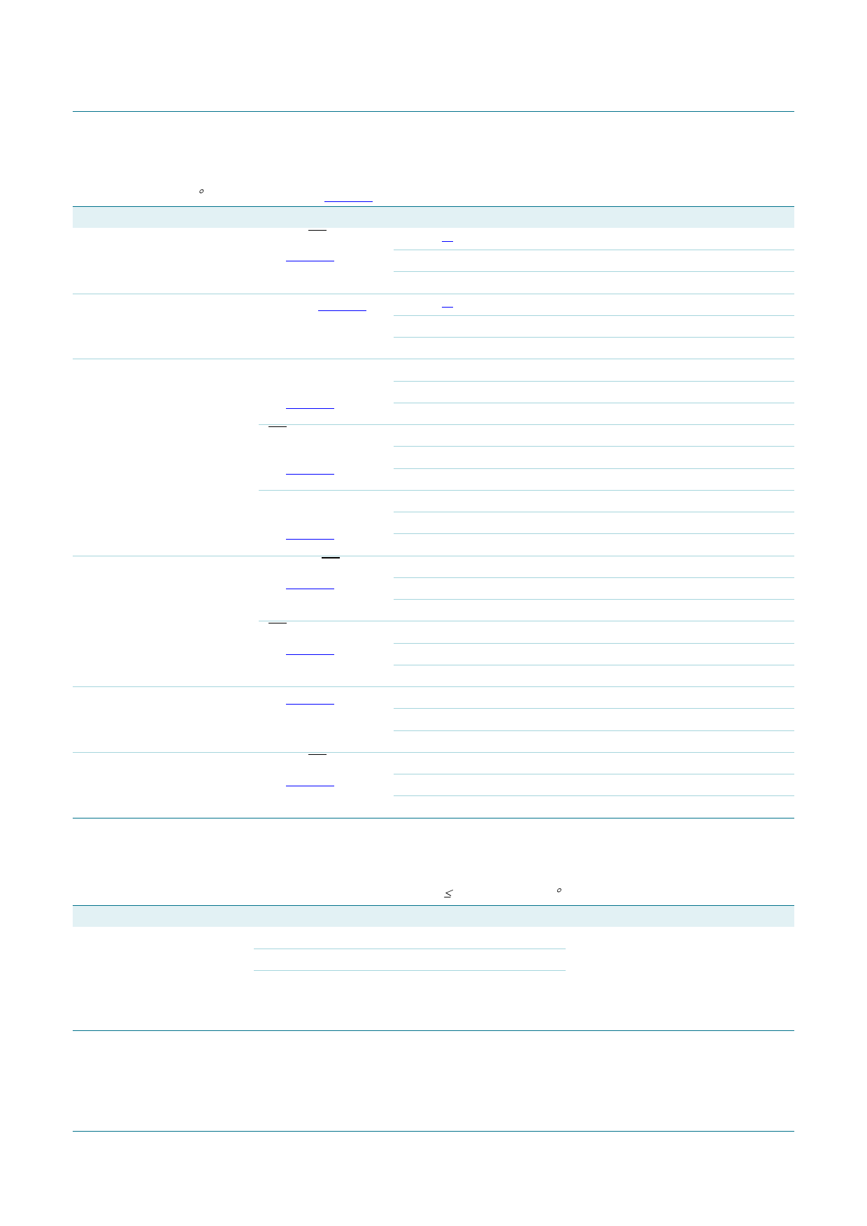
Table 7. Dynamic characteristics …continued
VSS = 0 V; Tamb = 25 C; for test circuit see Figure 6; unless otherwise specified.
Symbol Parameter
Conditions
VDD
Extrapolation formula
tPLH
LOW to HIGH
nCP0, nCP1 nQn; 5 V [1] 83 ns + (0.55 ns/pF)CL
propagation delay see Figure 5
10 V
39 ns + (0.23 ns/pF)CL
15 V
32 ns + (0.16 ns/pF)CL
tt
transition time
nQn; see Figure 5
5 V [1] 10 ns + (1.00 ns/pF)CL
10 V
9 ns + (0.42 ns/pF)CL
15 V
6 ns + (0.28 ns/pF)CL
tW
pulse width
nCP0 input LOW;
minimum width;
see Figure 5
5V
10 V
15 V
nCP1 input HIGH;
minimum width;
see Figure 5
5V
10 V
15 V
nMR input HIGH;
minimum width;
see Figure 5
5V
10 V
15 V
tsu
set-up time
nCP0 nCP1;
see Figure 5
5V
10 V
15 V
nCP1 nCP0;
see Figure 5
5V
10 V
15 V
trec
recovery time
see Figure 5
5V
10 V
15 V
fmax
maximum
frequency
nCP0, nCP1;
see Figure 5
5V
10 V
15 V
Min Typ Max Unit
-
110 220 ns
-
50 100 ns
-
40 80 ns
-
60 120 ns
-
30 60 ns
-
20 40 ns
60 30 -
ns
30 15 -
ns
20 10 -
ns
60 30 -
ns
30 15 -
ns
20 10 -
ns
30 15 -
ns
20 10 -
ns
16 8
-
ns
50 25 -
ns
30 15 -
ns
20 10 -
ns
50 25 -
ns
30 15 -
ns
20 10 -
ns
50 25 -
ns
30 15 -
ns
20 10 -
ns
8
16 -
MHz
15 30 -
MHz
20 40 -
MHz
[1] The typical values of the propagation delay and transition times are calculated from the extrapolation formulas shown (CL in pF).
Table 8. Dynamic power dissipation PD
PD can be calculated from the formulas shown. VSS = 0 V; tr = tf 20 ns; Tamb = 25 C.
Symbol Parameter
VDD
Typical formula for PD (W)
Where:
PD
dynamic power 5 V
PD = 850 fi + (fo CL) VDD2
fi = input frequency in MHz,
dissipation
10 V
PD = 3800 fi + (fo CL) VDD2
fo = output frequency in MHz,
15 V
PD = 10200 fi + (fo CL) VDD2
CL = output load capacitance in pF,
VDD = supply voltage in V,
(fo CL) = sum of the outputs.
HEF4520B
Product data sheet
All information provided in this document is subject to legal disclaimers.
Rev. 6 — 18 November 2011
© NXP B.V. 2011. All rights reserved.
6 of 14
Share Link: 