SL74HC4015D View Datasheet(PDF) - System Logic Semiconductor
Part Name
Description
View to exact match
SL74HC4015D Datasheet PDF : 6 Pages
| |||
SL74HC4015
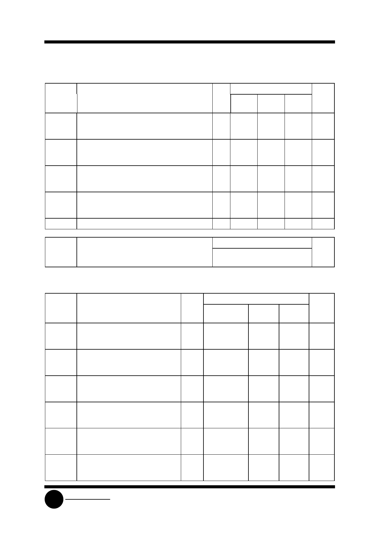
AC ELECTRICAL CHARACTERISTICS(CL=50pF,Input tr=tf=6.0 ns)
Symbol
Parameter
fmax Maximum Clock Frequency (50% Duty Cycle)
(Figure 2)
tPLH, tPHL Maximum Propagation Delay, Clock to Q (Figures
2 and 5)
tPHL Maximum Propagation Delay, Reset to Q (Figures
1 and 5)
tTLH, tTHL Maximum Output Transition Time, Any Output
(Figures 3 and 5)
CIN
Maximum Input Capacitance
VCC
Guaranteed Limit
V 25 °C to ≤85°C ≤125°C Unit
-55°C
2.0
6
4.8
4.5 30
24
6.0 35
28
4
MHz
20
24
2.0 175
220
265
ns
4.5 35
44
53
6.0 30
37
45
2.0 205
255
310
ns
4.5 41
51
62
6.0 35
43
53
2.0 75
95
110
ns
4.5 15
19
22
6.0 13
16
19
-
10
10
10
pF
Power Dissipation Capacitance (Per Latch)
CPD Used to determine the no-load dynamic power
consumption: PD=CPDVCC2f+ICCVCC
Typical @25°C,VCC=5.0 V
140
pF
TIMING REQUIREMENTS(CL=50pF,Input tr=tf=6.0 ns)
VCC
Symbol
Parameter
V
tsu
Minimum Setup Time, D to Clock
2.0
(Figure 4)
4.5
6.0
th
Minimum Hold Time, Clock to D
2.0
(Figure 4)
4.5
6.0
trec
Minimum Recovery Time, Reset to
2.0
Clock (Figure 1)
4.5
6.0
tw
Minimum Pulse Width, Reset (Figure 2.0
1)
4.5
6.0
tw
Minimum Pulse Width, Clock (Figure 2.0
4)
4.5
6.0
tr, tf Maximum Input Rise and Fall Times
2.0
(Figure 1)
4.5
6.0
Guaranteed Limit
25 °C to
-55°C
≤85°C ≤125°C Unit
50
65
75
ns
10
13
15
9.0
11
13
5
5
5
ns
5
5
5
5
5
5
5
5
5
ns
5
5
5
5
5
5
80
100
120
ns
16
20
24
14
17
20
80
100
120
ns
16
20
24
14
17
20
1000
1000
1000
ns
500
500
500
400
400
400
SLS
System Logic
Semiconductor
Share Link: 