A6850 View Datasheet(PDF) - Allegro MicroSystems
Part Name
Description
View to exact match
A6850 Datasheet PDF : 9 Pages
| |||
A6850
Dual Channel Switch Interface IC
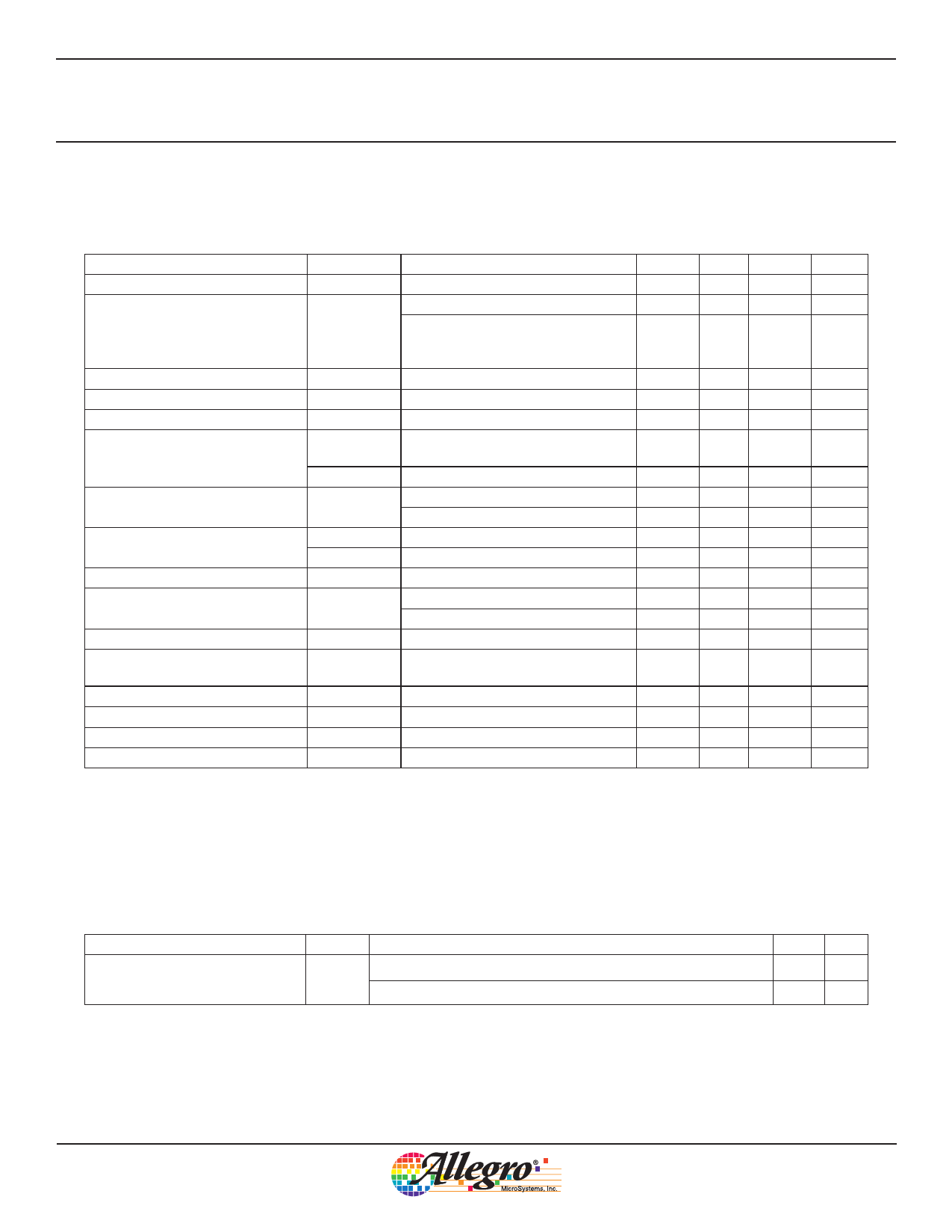
ELECTRICAL CHARACTERISTICS at TJ = -40 to +150°C (unless noted otherwise)
Characteristics
Symbol
Test Conditions
Min. Typ. Max. Units
Supply Input Voltage Range
Supply Input Quiescent Current
Power-Up Time1
OUTPUTx Source Resistance
OUTPUTx Leakage Current
SENSEx Output Current Offset2
SENSEx Voltage3
ENABLEx Input Voltage Range
ENABLEx Input Hysteresis
ENABLEx Current
VIN
IINQ
tON
RDS(on)
IOUTPUTQ
ISENSE(ofs)
ISENSEQ
VSENSEx
VENABLEH
VENABLEL
VENABLEhys
IENABLE
Operating mode, IOUTPUTx = 0 mA
Sleep mode:
ENABLE1 and ENABLE2 low
VOUTPUT1 = VOUTPUT2 = 0 V
IOUTPUTx = 20 mA
VOUTPUTx = 0 V; disabled
ISENSEx = (IOUTPUTx / 10) +
ISENSE(ofs), IOUTPUT = 2 mA to 20 mA
VSENSEx = 0 V; disabled
VIN > 7 V
VIN < 7 V
At least one output enabled
ENABLEx = 2.0 V
ENABLEx = 0.4 V
4.75
–
–
–
–
–
–100
–
0
0
2.0
–
150
–
–
–
26.5
V
–
5.0
mA
–
15
µA
–
20
µs
–
35
Ω
–
20
µA
–
100
µA
–
10
µA
–
6
V
– VIN – 1
V
–
–
V
–
0.4
V
–
350
mV
40
100
µA
8.0
20
µA
OUTPUT Current Limit
IOUTPUTM
25.0 35.0 45.0
mA
OUTPUT Reverse Bias Current
IOUTPUT(rvrs)
Reverse bias blocking: VIN = 4.75 V,
VOUTPUT = 26.5 V
–
500 750
µA
Overvoltage Protection Threshold
VOVP
Rising VIN
27.0
–
33.0
V
Overvoltage Protection Hysteresis VOVPhys
–
2.0
–
V
Thermal Shutdown Threshold
TTSD
Temperature Increasing
–
175
–
°C
Thermal Shutdown Hysteresis
TTSDhys
–
15
–
°C
1Delay from end of Sleep mode to outputs enabled.
2For input and output current specifications, negative current is defined as coming out of (sourced from) the specified device pin.
3User to ensure that VSENSEx remains within the specified range. If VSENSEx exceeds the maximum value, the device is self-protected by an
internal clamp, but not all parameters perform as specified.
THERMAL CHARACTERISTICS may require derating at maximum conditions, see application information
Characteristic
Symbol
Test Conditions*
Package Thermal Resistance
RθJA
4-layer PCB based on JEDEC standard
1-layer PCB with copper limited to solder pads
*Additional thermal data available on the Allegro Web site.
Value Units
80 ºC/W
140 ºC/W
Allegro MicroSystems, Inc.
115 Northeast Cutoff, Box 15036
Worcester, Massachusetts 01615-0036 (508) 853-5000
www.allegromicro.com
Share Link: 