SL2305ZI-1H View Datasheet(PDF) - SpectraLinear Inc
Part Name
Description
View to exact match
SL2305ZI-1H Datasheet PDF : 11 Pages
| |||
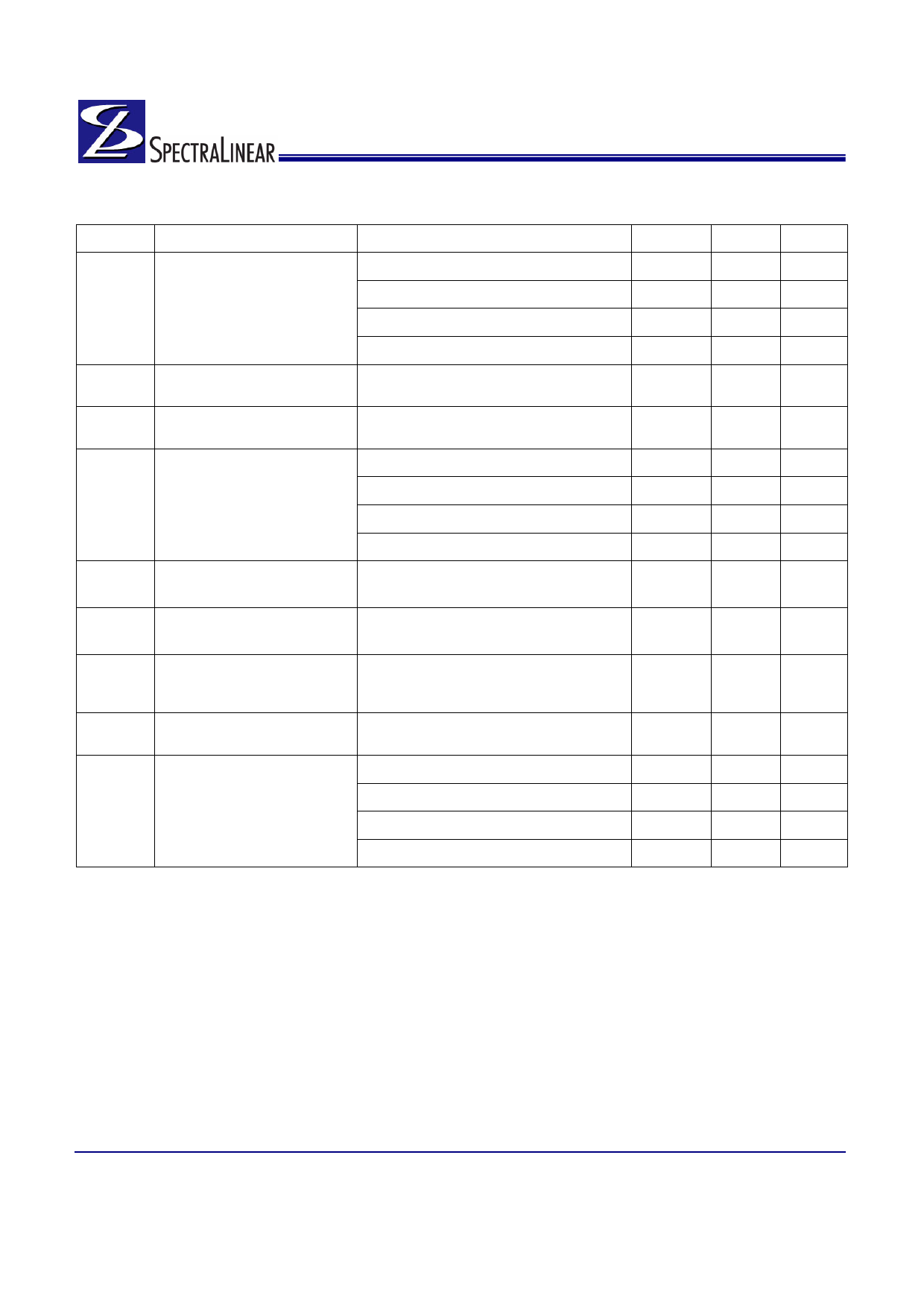
SL2305
Switching Specifications: Unless otherwise stated VDD=3.3V+/-10% and both C and I Grades
Symbol Description
Condition
Min
Max Unit
FMAX1
Maximum Frequency [1]
(Input=Output )
All Active PLL Modes
High drive (-1H). All outputs CL=15pF
10
High drive (-1H), All outputs CL=30pF
10
Standard drive, (-1), All outputs CL=15pf
10
140
MHz
100
MHz
100
MHz
Standard drive, (-1), All outputs CL=30pf
10
66
MHz
INDC
OUTDC
Input Duty Cycle
Output Duty Cycle[2]
tr/f
Rise, Fall Time (3.3V) [2]
(Measured at: 0.8 to 2.0V)
Measured at 1.4V, Fout=66MHz,
CL=15pF
Measured at 14V, Fout=66MHz,
CL=15pF
High drive (-1H), CL=10pF
High drive (-1H), CL=30pF
30
70
%
40
60
%
–
1.5
ns
–
1.8
ns
Standard drive (-1), CL=10pF
–
2.2
ns
Standard drive (-1), CL=30pF
–
2.5
ns
t1
Output-to-Output Skew[2]
All outputs CL=0 or equally loaded, -1 or
–
120
ps
(Measured at VDD/2)
-1H drives
t2
Device-to-Device Skew[2]
All outputs CL=0 or equally loaded, -1 or
(Measured at VDD/2)
-1H drives
–
400
ps
t3
Delay Time, CLKIN Rising
Measured at VDD/2
Edge to CLKOUT Rising
Edge[2]
–150
150
ps
tPLOCK PLL Lock Time[2]
Time from 90% of VDD to valid clocks on
all the output clocks
–
1.0
ms
CCJ
Cycle-to-cycle Jitter [2]
Fin=Fout=66 MHz, <CL=15pF, -1H drive
–
90
ps
Fin=Fout=66 MHz, <CL=15pF, -1 drive
–
100
ps
Fin=Fout=66 MHz, <CL=30pF, -1H drive
–
120
ps
Fin=Fout=66 MHz, <CL=30pF, -1 drive
–
140
ps
Notes:
1. For the given maximum loading conditions. See CL in Operating Conditions Table.
2. Parameter is guaranteed by design and characterization. Not 100% tested in production.
Rev 1.4, May 25, 2007
Page 6 of 11
Share Link: 