VP5511B View Datasheet(PDF) - Mitel Networks
Part Name
Description
View to exact match
VP5511B Datasheet PDF : 19 Pages
| |||
VP5311B/VP5511B
TIMING INFORMATION
Parameters
Master clock frequency (PXCK input)
PXCX pulse width, HIGH
PXCX pulse width, LOW
PXCX rise time
PXCX fall time
PD7-0 set up time
PD7-0 hold time
SC_SYNC set up time
SC_SYNC hold time
PAL_ID set up time
PAL_ID hold time
PAL_ID duration
Conditions
10% to 90% points
90% to 10% points
Output delay
PXCK to COMPSYNC
PXCK to CLAMP
Note: Timing reference points are at the 50% level. Digital C LOAD <40pF.
Symbol
fPXCK
tPWH; PXCK
tPWL; PXCK
tRP
tFP
tSU;PD
tHD;PD
tSU;SC_SYNC
tHD;SC_SYNC
tSU;PAL_ID
tHD;PAL_ID
tDUR;PAL_ID
tDOS
Min.
10
14.5
10
5
10
0
10
0
9
Typ.
27.0
Max.
TBD
TBD
25
Units
MHz
ns
ns
ns
ns
ns
ns
ns
ns
ns
ns
PXCX
periods
ns
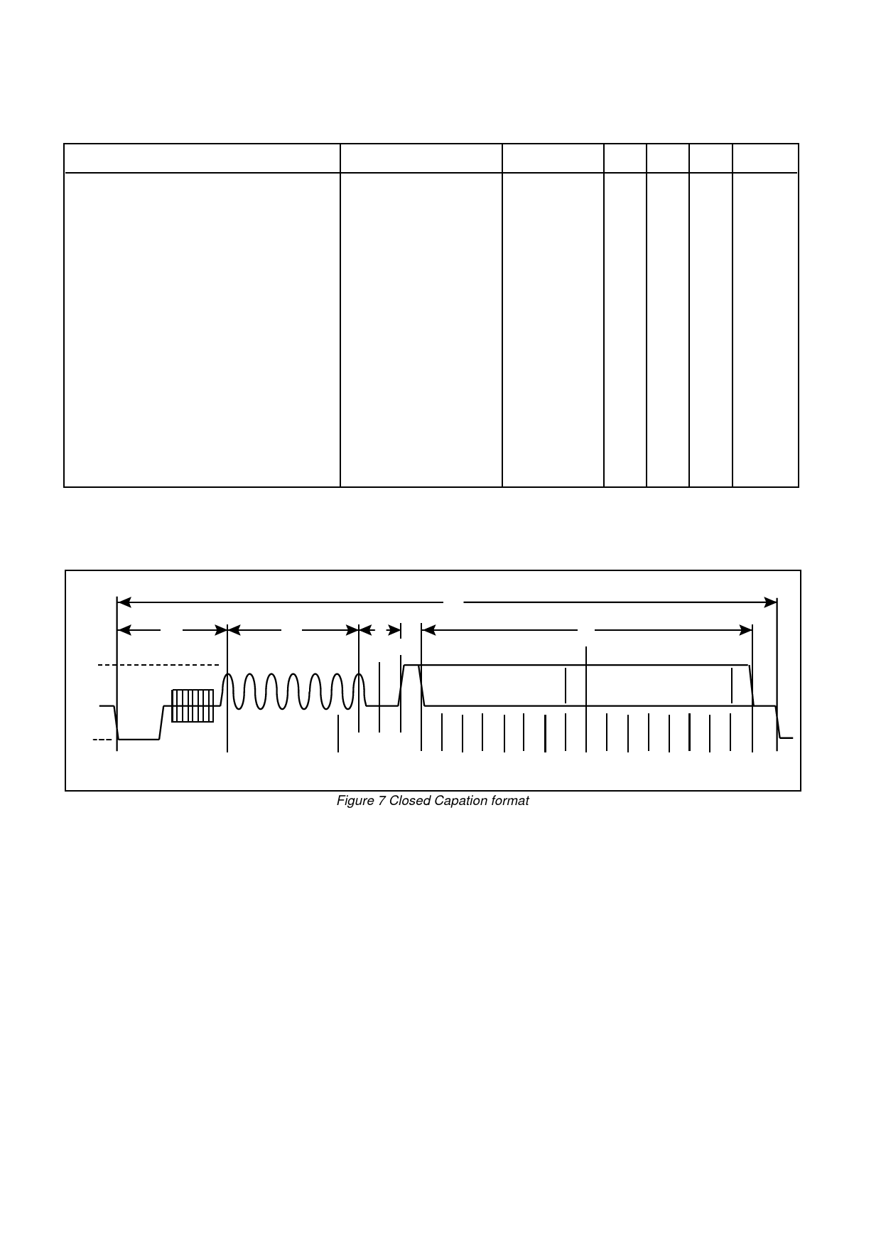
A
HSYNC COLOUR BURST
1
50
0
-40
IRE
B
CLOCK RUN-IN
CD
START BITS
13
H
DATA BYTE 1
E
P
DATA BYTE 2
P
S1 S2 S3 BIT0 BIT1 BIT2 BIT3 BIT4 BIT5 BIT6 BIT7 BIT0 BIT1 BIT2 BIT3 BIT4 BIT5 BIT6 BIT7
01000011
FRAME CODE
P = Parity Bit
Figure 7 Closed Capation format
12
Share Link: 