74LS95 View Datasheet(PDF) - Motorola => Freescale
Part Name
Description
View to exact match
74LS95 Datasheet PDF : 6 Pages
| |||
SN54 / 74LS95B
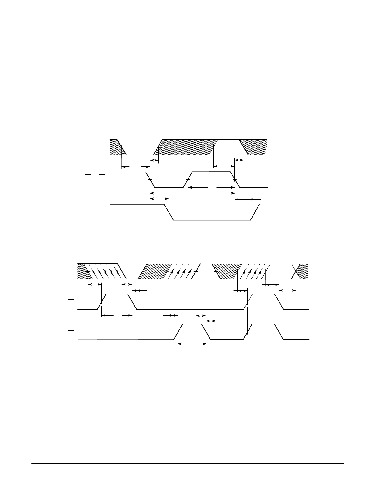
DESCRIPTION OF TERMS
SETUP TIME(ts) —is defined as the minimum time required
for the correct logic level to be present at the logic input prior to
the clock transition from HIGH to LOW in order to be recog-
nized and transferred to the outputs.
HOLD TIME (th) — is defined as the minimum time following
the clock transition from HIGH to LOW that the logic level must
be maintained at the input in order to ensure continued recog-
nition. A negative HOLD TIME indicates that the correct logic
level may be released prior to the clock transition from HIGH to
LOW and still be recognized.
AC WAVEFORMS
The shaded areas indicate when the input is permitted to change for predictable output performance.
D
CP1 or CP2
Q
1.3 V
1.3 V
th(L)
ts(L)
1.3 V
1.3 V
tPHL
l/fmax
1.3 V
1.3 V 1.3 V
ts(H)
1.3 V
tW
th(H)
*The Data Input is
(DS for CP1) or (Pn for CP2).
tPLH
1.3 V
Figure 1
(H
L ONLY)
S
1.3 V
(L
H ONLY)
1.3 V
(L
H ONLY)
STABLE
ts(H)
ts(L)
th(L)
ts(L)
ts(H)
th(LĂORĂH)
CP1
1.3 V
CP2
1.3 V
1.3 V
tW
ts(L)
ts(H)
th(H)
1.3 V
1.3 V
1.3 V
tW
1.3 V
1.3 V
Figure 2
FAST AND LS TTL DATA
5-174
Share Link: 