PSB4860 View Datasheet(PDF) - Siemens AG
Part Name
Description
View to exact match
PSB4860 Datasheet PDF : 250 Pages
| |||
PSB 4860
Overview
Table 1
32
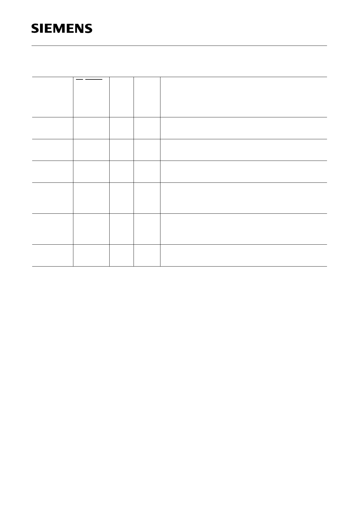
Pin Definitions and Functions
W/FWE O
H2) ARAM, DRAM:
Write signal for all memory banks.
Flash Memory:
Write signal for Flash Memory.
31
FRDY I
-
Flash Memory Ready
Input for Ready/Busy signal of Flash Memory
5
OSC1 I
-
Auxiliary Oscillator:
6
OSC2 O
Z
Oscillator loop for 32.768 kHz crystal.
8
CLK
I
-
Alternative AFECLK Source
13,824 MHz
2
XTAL1 I
-
Oscillator:
3
XTAL2 O
Z
XTAL1: External clock or input of oscillator loop.
XTAL2: output of oscillator loop for crystal.
37
SPS0
O
L
Multipurpose Outputs:
38
SPS1
O
L
General purpose, speakerphone, address lines
or status
56
RO
O-
Reserved Output
Must be left open.
1) These lines are driven low with 125 µA until the mode (address lines or auxiliary port) is defined.
2) These lines are driven high with 70 µA during reset.
Semiconductor Group
17
10.97
Share Link: 