NT68F62U View Datasheet(PDF) - Unspecified
Part Name
Description
View to exact match
NT68F62U Datasheet PDF : 57 Pages
| |||
NT68F62
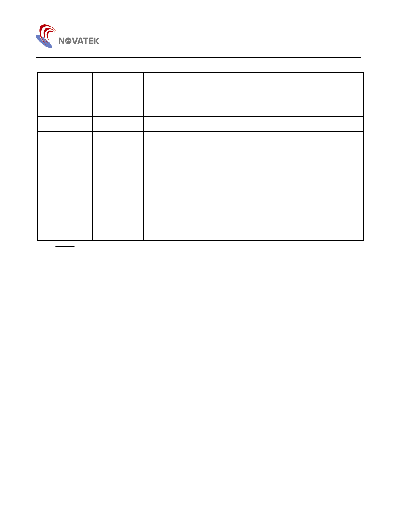
Pin Description (continued)
Pin No.
40 Pin 42 Pin
Designation
37
39
DAC4/SCL1
Reset Init.
DAC4
I/O
Description
O
Open drain 5V, D/A converter output 4, shared with the
open drain SCL1 line of IIC bus, Schmitt Trigger buffer
38
40
DAC3
O Open drain 5V, D/A converter output 3
39
41
HSYNCI
Debouncing & Schmitt Trigger input pin for video horizontal
I sync signal, internal pull high, shared with the composite
sync input
Debouncing & Schmitt trigger input pin for video vertical
40
42
VSYNCI/INTV
VSYNCI
I
sync signal, internal pull high, shared with the input pin of
the external interrupt source, intv, with Schmitt Trigger,
selectable triggered and internal pulled up 22KΩ resistor
-
6
P40
I/O
Bi-directional I/O pin with internal pulled up 22KΩ resistor,
only 42 pin S-DIP available
-
37
P41
I/O
Bi-directional I/O pin with internal pulled up 22KΩ resistor,
only 42 pin S-DIP available
* This RESET pin must be pulled high by an external pulled-up resistor (5KΩ suggestion), or it will remain at low voltage to
continually rest system.
5
Share Link: 