B5S162861 View Datasheet(PDF) - STMicroelectronics
Part Name
Description
View to exact match
B5S162861 Datasheet PDF : 9 Pages
| |||
B5S162861
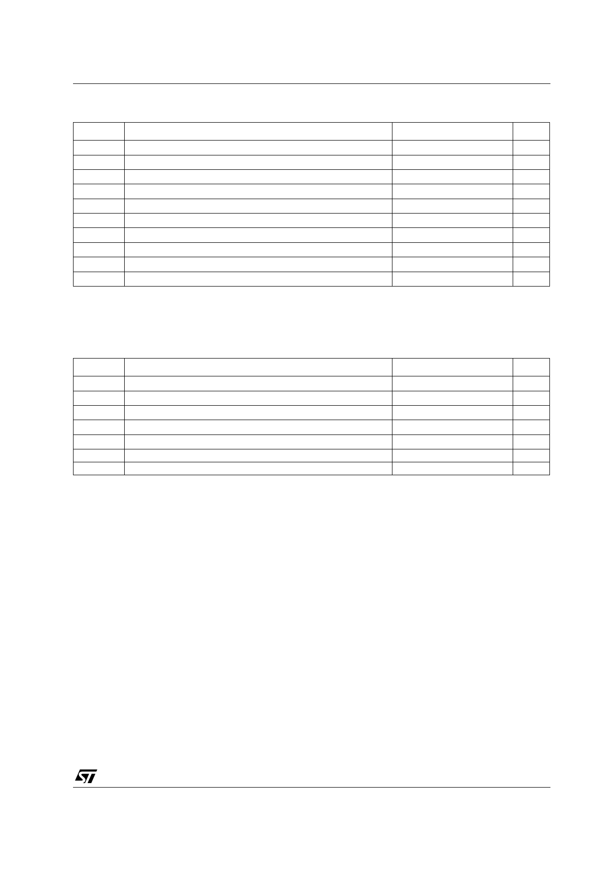
ABSOLUTE MAXIMUM RATINGS
Symbol
Parameter²
Value
Unit
VCC Supply Voltage
-0.5 to +7.0
V
VI
DC Switch and Control Pin Voltage
-0.5 to +7.0
V
VO
DC Output Voltage (VCC = 0V) (note 1)
-0.5 to +7.0
V
VO
DC Output Voltage (VI/O=Gnd)
-0.5 to +7.0
V
IIK
DC Input Diode Current (VI/O < 0V)
- 50
mA
IOK
DC Output Diode Current (note 2)
- 50
mA
IO
DC Output Current (note 3)
128
mA
ICC or IGND DC VCC or Ground Current per Supply Pin
± 100
mA
Tstg
Storage Temperature
-65 to +150
°C
TL
Lead Temperature (10 sec)
300
°C
Absolute Maximum Rating are those value beyond which damage to the device may occour. Functional operation under these condition is
not implied
1) IO absolute maximum rating must be observed
2) VO < GND, VO > VCC
3) Not more than one output should be tested at one time. Duration of the test should not exceed one second.
RECOMMENDED OPERATING CONDITIONS
Symbol
Parameter
VCC Supply Voltage
VI
Input Voltage
VO
Output Voltage (VCC = 0V)
VO
Output Voltage
Top
Operating Temperqture
dt/dv Switch Input Rise and Fall Time
dt/dv Control Input Rise and Fall Time (note 1)
1) VIN from 0.8V to 2V at VCC = 3.0V
Value
4 to 5.5
0 to 5.5
0 to 5.5
0 to 5.5
-55 to 125
0 to DC
0 to 10
Unit
V
V
V
V
°C
ns/V
ns/V
3/9
Share Link: 