AG103(2004) View Datasheet(PDF) - WJ Communications => Triquint
Part Name
Description
View to exact match
AG103 Datasheet PDF : 5 Pages
| |||
AG103
High Dynamic Range Gain Block
The Communications Edge TM
Product Information
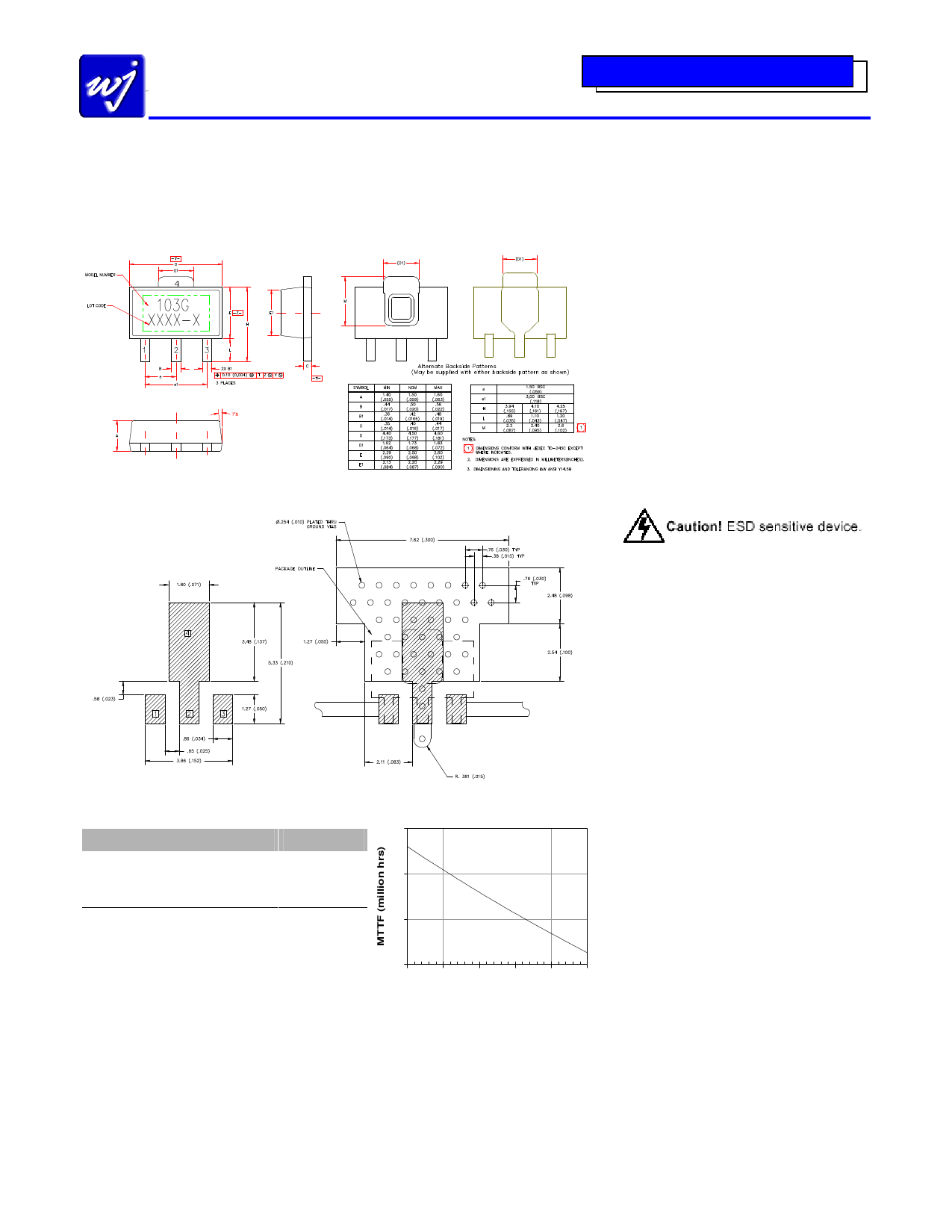
AG103 (SOT-89 Package) Mechanical Information
This package may contain lead-bearing materials. The plating material on the leads is SnPb.
Outline Drawing
Product Marking
The AG103 will be marked with an “AG103”
designator. An alphanumeric lot code
(“XXXX-X”) is also marked below the part
designator on the top surface of the package.
Tape and reel specifications for this part are
located on the website in the “Application
Notes” section.
MSL / ESD Rating
Land Pattern
ESD Rating: Class 1B
Value:
Passes 500V to <1000V
Test:
Human Body Model (HBM)
Standard: JEDEC Standard JESD22-A114
ESD Rating: Class IV
Value:
Passes 1000V to <2000V
Test:
Charged Device Model (CDM)
Standard: JEDEC Standard JESD22-C101
MSL Rating: Level 3 at +235° C convection reflow
Standard: JEDEC Standard J-STD-020
Mounting Config. Notes
Thermal Specifications
Parameter
Rating
MTTF vs. GND Tab Temperature
1000
1. Ground / thermal vias are critical for the proper
performance of this device. Vias should use a .35mm
(#80 / .0135”) diameter drill and have a final plated
thru diameter of .25 mm (.010”).
2. Add as much copper as possible to inner and outer
layers near the part to ensure optimal thermal
performance.
3. Mounting screws can be added near the part to fasten
the board to a heatsink. Ensure that the ground /
thermal via region contacts the heatsink.
4. Do not put solder mask on the backside of the PC board
in the region where the board contacts the heatsink.
5. RF trace width depends upon the PC board material
and construction.
6. Use 1 oz. Copper minimum.
7. All dimensions are in millimeters (inches). Angles are
in degrees.
Operating Case Temperature
Thermal Resistance, Rth (1)
Junction Temperature, Tjc (2)
-40 to +85°C
59° C / W
100
129° C
10
1. The thermal resistance is referenced from the hottest
part of the junction to the ground tab (pin 4).
2. This corresponds to the typical biasing condition of
+5V, 150 mA at an 85°C case temperature. A
minimum MTTF of 1 million hours is achieved for
junction temperatures below 160 °C.
1
60 70 80 90 100 110
Tab Temperature (°C)
Specifications and information are subject to change without notice.
WJ Communications, Inc • Phone 1-800-WJ1-4401 • FAX: 408-577-6621 • e-mail: sales@wj.com • Web site: www.wj.com
September 2004
Share Link: 