A62S7308BV View Datasheet(PDF) - AMIC Technology
Part Name
Description
View to exact match
A62S7308BV Datasheet PDF : 17 Pages
| |||
AC Test Conditions
Input Pulse Levels
Input Rise and Fall Time
Input and Output Timing Reference Levels
Output Load
0V to 3V
5 ns
1.5V
See Figures 1 and 2
A62S7308B Series
TTL
TTL
CL
30pF
CL
5pF
* Including scope and jig.
* Including scope and jig.
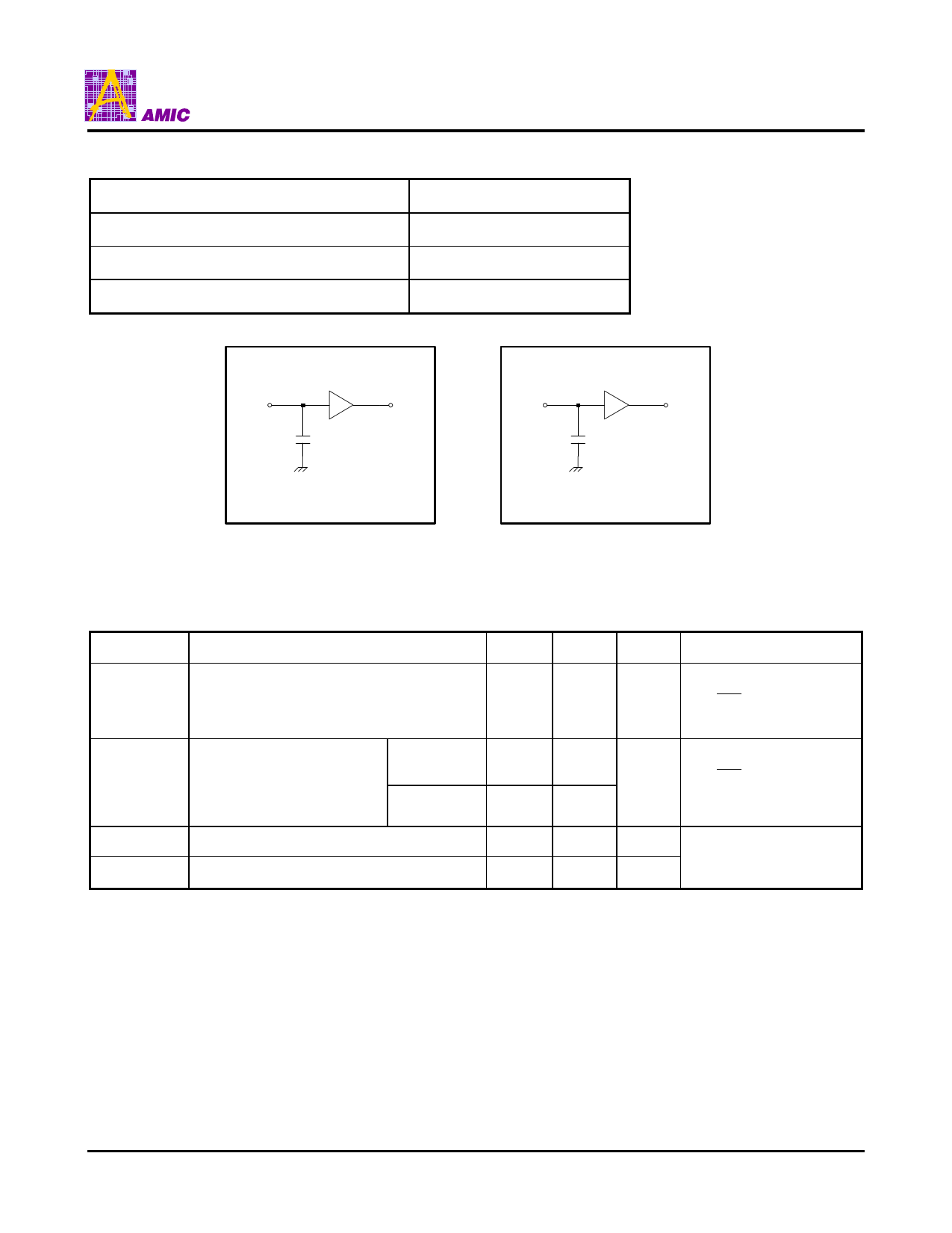
Figure 1. Output Load
Figure 2. Output Load for tCLZ1,
tCLZ2, tOHZ, tOLZ, tCHZ1,
tCHZ2, tWHZ, and tOW
Data Retention Characteristics (TA = 0°C to + 70°C or -25°C to 85°C)
Symbol
Parameter
Min. Max. Unit
Conditions
VDR
VCC for Data Retention
2.0
3.6
CE2 ≤ 0.2V,
V
{or CE1 ≥ VCC - 0.2V,
CE2 ≥ VCC - 0.2V
ICCDR
Data Retention Current
S-Version
-
SI-Version
-
2*
VCC = 2.0V, CE2 ≤ 0.2V,
5**
µA
{or CE1 ≥ VCC - 0.2V
CE2 ≥ VCC - 0.2V
tCDR
Chip Disable to Data Retention Time
tR
Operation Recovery Time
0
-
ns
See Retention Waveform
tRC
-
ns
* A62S7308B-55S/70S ICCDR: Max. 1µA at TA = 0°C to + 40°C
** A62S7308B-55SI/70SI ICCDR: Max. 1µA at TA = 0°C to + 40°C
PRELIMINARY
(March, 2001, Version 0.2)
10
AMIC Technology, Inc.
Share Link: 