SAA8110G/C1 View Datasheet(PDF) - Philips Electronics
Part Name
Description
View to exact match
SAA8110G/C1 Datasheet PDF : 36 Pages
| |||
Philips Semiconductors
Digital Signal Processor (DSP) for
cameras
Preliminary specification
SAA8110G
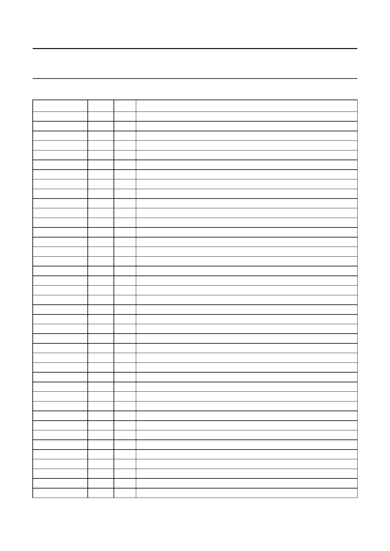
PINNING
SYMBOL
VDDD(C1)
CLK1
VSYNCIN
HSYNCIN
FIIN
VSSD(C1)
CCD9
CCD8
CCD7
CCD6
CCD5
CCD4
CCD3
CCD2
CCD1
CCD0
VSSD(C2)
SCLK
VSSA(CD)
CDACOUT
CDACRBIAS
VDDA(CD)
SDATA
STROBE
SMP
P0
P1
SIS
VDDD(C2)
RESET
T2
T1
T0
VSSA(OB)
OUT3
VDDA(O3)
OUT2
VDDA(O2)
OUT1
VDDA(O1)
1997 Jun 13
PIN I/O
DESCRIPTION
1
I digital supply 1 for digital core and CLK1 related peripherals
2
I system- or pixel clock
3
I vertical synchronization input
4
I horizontal synchronization input
5
I field identification signal input
6
I digital ground 1 for digital core and CLK1 related peripherals
7
I (preprocessed) AD-converted CDD-signal bit 9 (MSB)
8
I (preprocessed) AD-converted CDD-signal bit 8
9
I (preprocessed) AD-converted CDD-signal bit 7
10
I (preprocessed) AD-converted CDD-signal bit 6
11
I (preprocessed) AD-converted CDD-signal bit 5
12
I (preprocessed) AD-converted CDD-signal bit 4
13
I (preprocessed) AD-converted CDD-signal bit 3
14
I (preprocessed) AD-converted CDD-signal bit 2
15
I (preprocessed) AD-converted CDD-signal bit 1
16
I (preprocessed) AD-converted CDD-signal bit 0 (LSB)
17
I digital ground 2 for digital core and CLK1 related peripherals
18
O serial clock to TDA8786
19
I analog ground for control DAC
20
O output control DAC
21
I pin to connect external bias resistor for control DAC
22
I analog supply for control DAC
23
O serial data to TDA8786
24
O strobe to TDA8786
25
O switch mode pulse for DC-DC
26
O quasi-static control output pin 0
27
O quasi-static control output pin 1
28
I SNERT/I2C-bus select input signal
29
I digital supply 2 for digital core and CLK1 related peripherals
30
I reset input
31
I test mode control signal bit 2
32
I test mode control signal bit 1
33
I test mode control signal bit 0
34
I analog ground for the three output buffers
35
O output buffer 3 (R, V or CVBS)
36
I analog supply for output buffer OUT3
37
O output buffer 2 (B, U or C)
38
I analog supply for output buffer OUT2
39
O output buffer 1 (G or Y)
40
I analog supply for output buffer OUT1
5
Share Link: 