WM8580 View Datasheet(PDF) - Wolfson Microelectronics plc
Part Name
Description
View to exact match
WM8580 Datasheet PDF : 97 Pages
| |||
WM8580
PIN
NAME
TYPE
DESCRIPTION
47
48
Notes :
VOUT3L
VOUT3R
Analogue Output
Analogue Output
DAC channel 3 left output
DAC channel 3 right output
1. Digital input pins have Schmitt trigger input buffers. Pins 32, 33, 34 are 5V tolerant.
2. In hardware control mode, pin 30 is used for UNLOCK flag output.
3. In hardware control mode, pin 31 is used for NON_AUDIO flag output.
Production Data
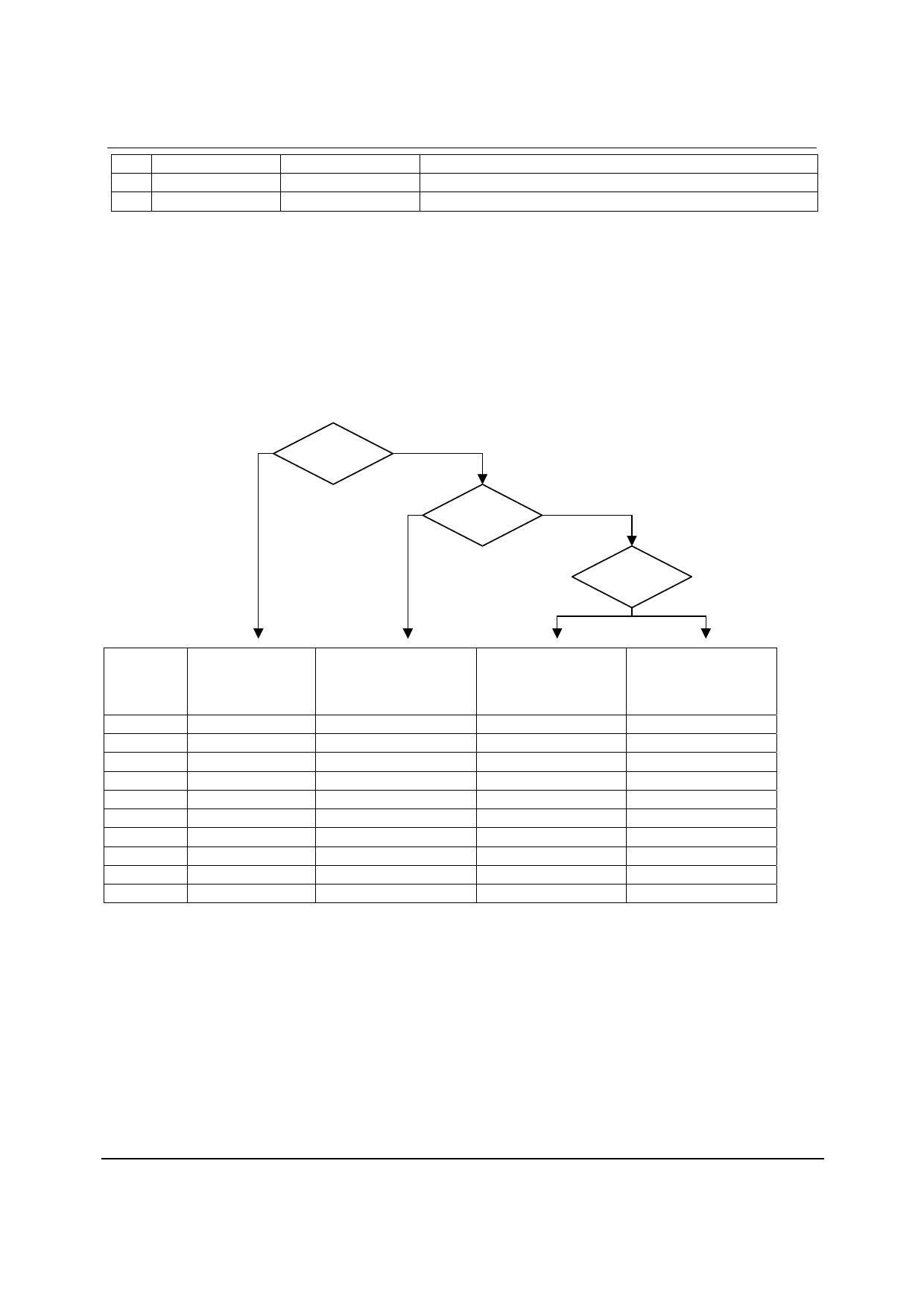
MULTI-FUNCTION PINS
The WM8580 has 8 Multi-Function Input/Output pins (MFP1 etc.). The function and direction (input/output) of these pins
are configured using the HWMODE input pin and software register control as shown below. If HWMODE is set, the MFPs
have the function shown in column 1 of Table 1. If HWMODE is not set, and the register SAIF_EN is set, the MFPs have
the function shown in column 2. Otherwise, the GPOnOP registers determine the MFP function as shown in columns 3 and
4.
Y HWMODE = 1 N
Y SAIF_EN = 1 N
GPIOnOP
PIN NAME
MFP1
MFP2
MFP3
MFP4
MFP5
MFP6
MFP7
MFP8
MFP9
MFP10
HARDWARE
CONTROL MODE
FUNCTION
1
PAIFTX_BCLK
ADCMCLK
DR1
DR2
DR3
DR4
ALLPD
C
SFRM_CLK
192BLK
SECONDARY AUDIO
INTERFACE FUNCTION
2
n/a1
n/a1
n/a1
n/a1
n/a1
SAIF_BCLK
SAIF_LRCLK
SAIF_DIN
SAIF_DOUT
n/a1
Table 1 Multi-Function Pin Configuration
S/PDIF INPUT &
INDEPENDENT
CLOCKING
3
PAIFTX_BCLK2
ADCMCLK3
SPDIFIN2
SPDIFIN3
SPDIFIN4
GPO6
GPO7
GPO8
GPO9
GPO10
GENERAL PURPOSE
OUTPUT FUNCTION
4
GPO1
GPO2
GPO3
GPO4
GPO5
GPO6
GPO7
GPO8
GPO9
GPO10
Notes:
1. These pins are not used as part of the Secondary Audio Interface, so their function is that of either Column 3 or
Column 4.
2. MFP1 usage can be described as follows:
IF (ADC_CLKSEL = MCLK) AND (PAIFTXMS_CLKSEL = MCLK) THEN
MFP1 = GPO1;
ELSE
MFP1 = PAIFTX_BCLK ; (default)
w
PD Rev 4.3 August 2007
6
Share Link: 