VV6501 View Datasheet(PDF) - STMicroelectronics
Part Name
Description
View to exact match
VV6501 Datasheet PDF : 60 Pages
| |||
VV6501
Functional Description
3 Functional Description
The first three sections of this chapter detail the main blocks in the device:
q Video
q Audio
q Power management
The final section describes the device level operating modes including suspend.
3.1 Video block
3.1.1
Overview
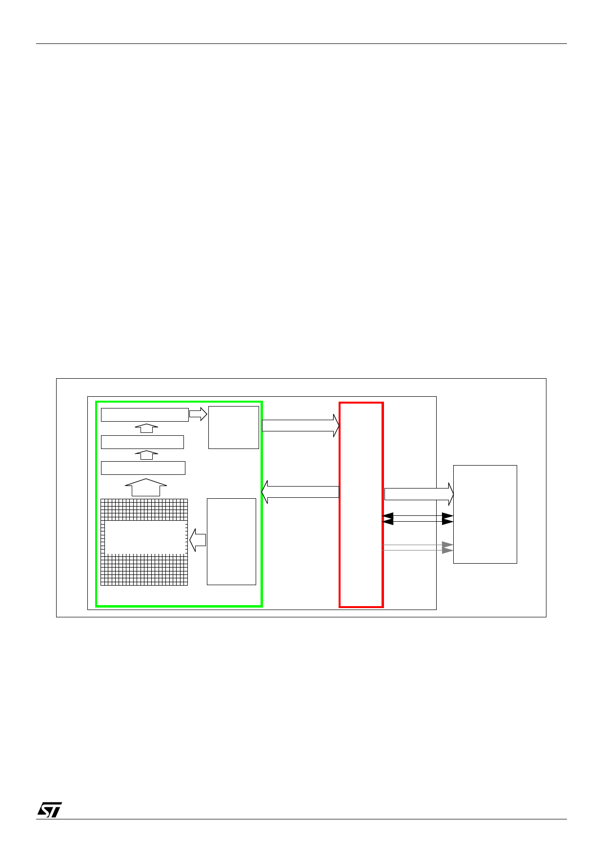
The analog core of the video block contains a VGA sized pixel array. The integration time and
access for a row of pixels is controlled by the Y-address block. The row of pixels being read is
converted using a 10-bit in-column ADC. The digitised data is readout into the digital block for
formatting. The 10-b data is transferred to the co-processor over a 5-wire digital bus as two 5-b
nibbles.
The exposure or integration time for the pixel array is calculated by the external co-processor and
delivered to the sensor using the I2C interface.
Figure 4: Overview of video block
SRAM line store
X-Address
Column ADC
VGA
photodiode
array
Readout
structure
10-b image data
Timing & control
Digital
logic
10-b image
data D[4:0]
I2C
Y address
FST, QCK
Coprocessor
Data synchronization can be achieved either by using the embedded codes within the data stream
or by making use of the dedicated FST and QCK pins.
9/60
Share Link: 