VP531E View Datasheet(PDF) - Mitel Networks
Part Name
Description
View to exact match
VP531E Datasheet PDF : 16 Pages
| |||
VP531E/VP551E
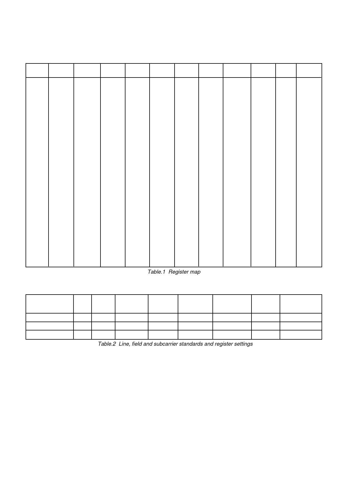
REGISTERS MAP
See Register Details for further explanations.
ADDRESS REGISTER
hex
NAME
7
6
5
4
3
2
DEFAULT
1
0
R/W
hex
BAR
RA7
RA6
RA5
RA4
RA3
RA2
RA1
RA0
W
00 PART ID2 ID17
ID16
ID15
ID14
ID13
ID12
ID11
ID10
R
13
01 PART ID1 ID0F
ID0E
ID0D
ID0C
ID0B
ID0A
ID09
ID08
R
66
02 PART ID0 ID07
ID06
ID05
ID04
ID03
ID02
ID01
ID00
R
57
03
REV ID
REV7
REV6
REV5
REV4
REV3
REV2
REV1
REV0
R
05
SLH&V
04
GCR
-
-
YCDELAY RAMPEN
-
-
VFS1
VFS0
R/W
00
05
VOCR
-
CLAMPDIS CHRBW SYNCDIS BURDIS LUMDIS CHRDIS PEDEN
R/W
00
06
HANC
-
-
DFI2
DFI1
DFI0 Reserved Reserved ACTREN
*
00
07
ANCID
AN7
AN6
AN5
AN4
AN3
AN2
AN1
PARITY R/W
00
08
SC_ADJ
SC7
SC6
SC5
SC4
SC3
SC2
SC1
SC0
R/W
9C
09
FREQ2
FR17
FR16
FR15
FR14
FR13
FR12
FR11
FR10
R/W
87
0A
FREQ1
FR0F
FR0E
FR0D
FR0C
FR0B
FR0A
FR09
FR08
R/W
C1
0B
FREQ0
FR07
FR06
FR05
FR04
FR03
FR02
FR01
FR00
R/W
F1
0C SCHPHM
-
-
-
-
-
-
-
SCH8
R/W
00
0D
SCHPHL SCH7
SCH6
SCH5
SCH4
SCH3
SCH2
SCH1
SCH0
R/W
00
0E to 1F Reserved
20
GPPCTL
CTL7
CTL6
CTL5
CTL4
CTL3
CTL2
CTL1
CTL0
W
FF
21
GPPRD
RD7
RD6
RD5
RD4
RD3
RD2
RD1
RD0
R
-
22
GPPWR
WR7
WR6
WR5
WR4
WR3
WR2
WR1
WR0
W
00
23 to EF Not used
F0 to F7 Reserved
F8
HSOFFL HSOFF7 HSOFF6 HSOFF5 HSOFF4 HSOFF3 HSOFF2 HSOFF1 HS0FF0 R/W
7E
F9
HSOFFM
-
-
-
-
-
-
HSOFF9 HSOFF8 R/W
00
FB
SLAVE1 NCORSTD VBITDIS VSMODE F_SWAP SL_HS1 SL_HS0 HCNT9 HCNT8
R/W
00
FC
SLAVE2 HCNT7 HCNT6 HCNT5 HCNT4 HCNT3 HCNT2
HCNT1 HCNT0
R/W
00
FD
GPSDAC
REGISTER RESERVED FOR
TEST
R/W
FE
GPSTST
REGISTER RESERVED FOR
TEST
R/W
FF
GPSCTL FSC4SEL GENDITH GENLKEN NOLOCK PALIDEN TSURST CHRMCLIP TRSEL
R/W
00
Table.1 Register map
NOTE * For register HANC, bits 3, 4 and 5 are read only. Bits 1 and 2 are reserved. N/A = not applicable.
For register PART ID0 the VP551 value is AA
Standard
Lines/ Field
field freq. HZ
NTSC (default) 525 59.94
PAL-B, D, G, H, I 625 50
PAL-N (Argentina) 625 50
Number of
pixels/line
at 27MHz
1716
1728
1728
Horizontal
freq. kHz.
fH
15.734266
15.625000
15.625000
Subcarrier
freq. kHz.
fSC
3.57954545
fSC/fH
(455/2)
SC_ADJ
register
hex
xx
4.43361875 (1135/4+1/625) 9C
3.58205625 (917/4+1/625) 57
FREQ2-0
registers hex
87 C1 F1
A8 26 2B
87 DA 51
xx = don’t care.
Table.2 Line, field and subcarrier standards and register settings
The calculation of the FREQ register value is according to the following formula:-
FREQ = (226 x fSC/fH) /(number of pixels/line) hex
NTSC value is rounded UP from the decimal number. PAL-B, D, G, H, I and N (Argentina) are rounded DOWN. The SC_ADJ
value is derived from the adjustment needed to be added after 8 fields to ensure accuracy of the Subcarrier frequency. Note the
SC_ADJ value of 9C required for PAL-B, D, G, H, I, is different to the default state of the register.
In NTSC the NCO is reset at the end of every line, this can be disabled by setting the NCORSTD bit in SLAVE1, this allows the
VP531/VP551 to cope with line lengths that are not exactly as specified in REC656.
6
Share Link: 