UPC8129GR-E1 View Datasheet(PDF) - NEC => Renesas Technology
Part Name
Description
View to exact match
UPC8129GR-E1
NEC => Renesas Technology

UPC8129GR-E1 Datasheet PDF : 28 Pages
| |||
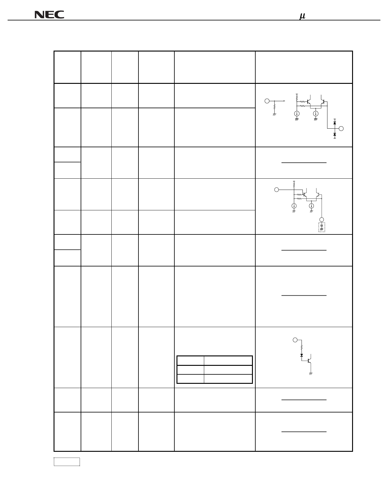
µPC8129GR
PIN EXPLANATION
Pin No.
8
9
Symbol
LO1in
LO1in b
Supply
Voltage
(V)
–
–
Pin
Voltage
Typ. (V)
@VCC = 3 V
0
2.3
Description
Lo1 input for phase shifter.
This input impedance is 50 Ω
matched internally.
Bypass of Lo1 input.
This pin is grounded through
internal capacitor.
Equivalent Circuit
8
50 Ω
9
10
GND for
0
Modulator
11
–
Connect to the ground with
minimum inductance.
Track length should be kept as
short as possible.
12
LO2in b
–
1.9
Bypass of Lo2 input.
Grounded through external
13
capacitor.
13
LO2in
–
1.9
Lo2 input of Up-converter.
12
This pin is high impedance input.
14
GND for
0
Up-con.
17
–
Connect to the ground with
minimum inductance.
Track length should be kept as
short as possible.
15
VAGC
0 to VCC
–
Input for AGC amplifier.
Total Output Power can be
controlled by changing input
voltage.
And as external series resistance
(RAGC) connecting, a slope of
AGC curve can be changed by
the resistance (RAGC).
16
Power
0 to VCC
–
Power save control pin can be
Save
controlled ON/OFF state with
16
bias as follows;
VPS (V)
2 to VCC
0 to 0.5
STATE
ON (Active Mode)
OFF (Sleep Mode)
19
VCC for
2.7 to 5.5
–
Up-
converter
20
VCC for
2.7 to 5.5
–
Modulator
Supply voltage pin for Up-
converter.
Supply voltage pin for modulator.
Internal regulator can be kept
stable condition of supply bias
against the variable
temperature or VCC.
: Externally
Data Sheet P12781EJ2V0DS00
9
Share Link: