IDT61298SA12Y(2007) View Datasheet(PDF) - Integrated Device Technology
Part Name
Description
View to exact match
IDT61298SA12Y Datasheet PDF : 8 Pages
| |||
IDT61298SA
CMOS Static RAM 256K (64K x 4-Bit)
Recommended Operating
Temperature and Supply Voltage
Grade
Temperature
GND
Vcc
Commercial
0OC to +70OC
0V
5V ± 10%
2971 tbl 05
Commercial Temperature Range
Recommended DC Operating
Conditions
Symbol
Parameter
Min. Typ. Max. Unit
VCC Supply Voltage
4.5 5.0
5.5
V
GND Ground
00
0
V
VIH Input High Voltage
2.2 ____ VCC + 0.5V V
VIL Input Low Voltage
-0.5(1) ____
0.8
V
NOTE:
2971 tbl 06
1. VIL (min.) = –1.5V for pulse width less than 10ns, once per cycle.
DC Electrical Characteristics(1)
(VCC = 5V ± 10%, VLC = 0.2V, VHC = VCC - 0.2V)
Symbol
Parameter
ICC Dynamic Operating Current CS < VIL, Outputs
Open, VCC = Max., f = fMAX(2)
ISB Standby Power Supply Current (TTL Level)
CS > VIH, VCC = Max., Outputs Open, f = fMAX(2)
ISB1 Full Standby Power Supply Current (CMOS Level)
CS > VHC, VCC = Max., f = 0(2), VIN < VLC or VIN > VHC
NOTES:
1. All values are maximum guaranteed values.
2. fMAX = 1/tRC (all address inputs are cycling at fMAX); f = 0 means no address input lines are changing.
61298SA12
Com'l.
160
50
20
61298SA15
Com'l.
Unit
140
mA
45
mA
20
mA
2971 tbl 07
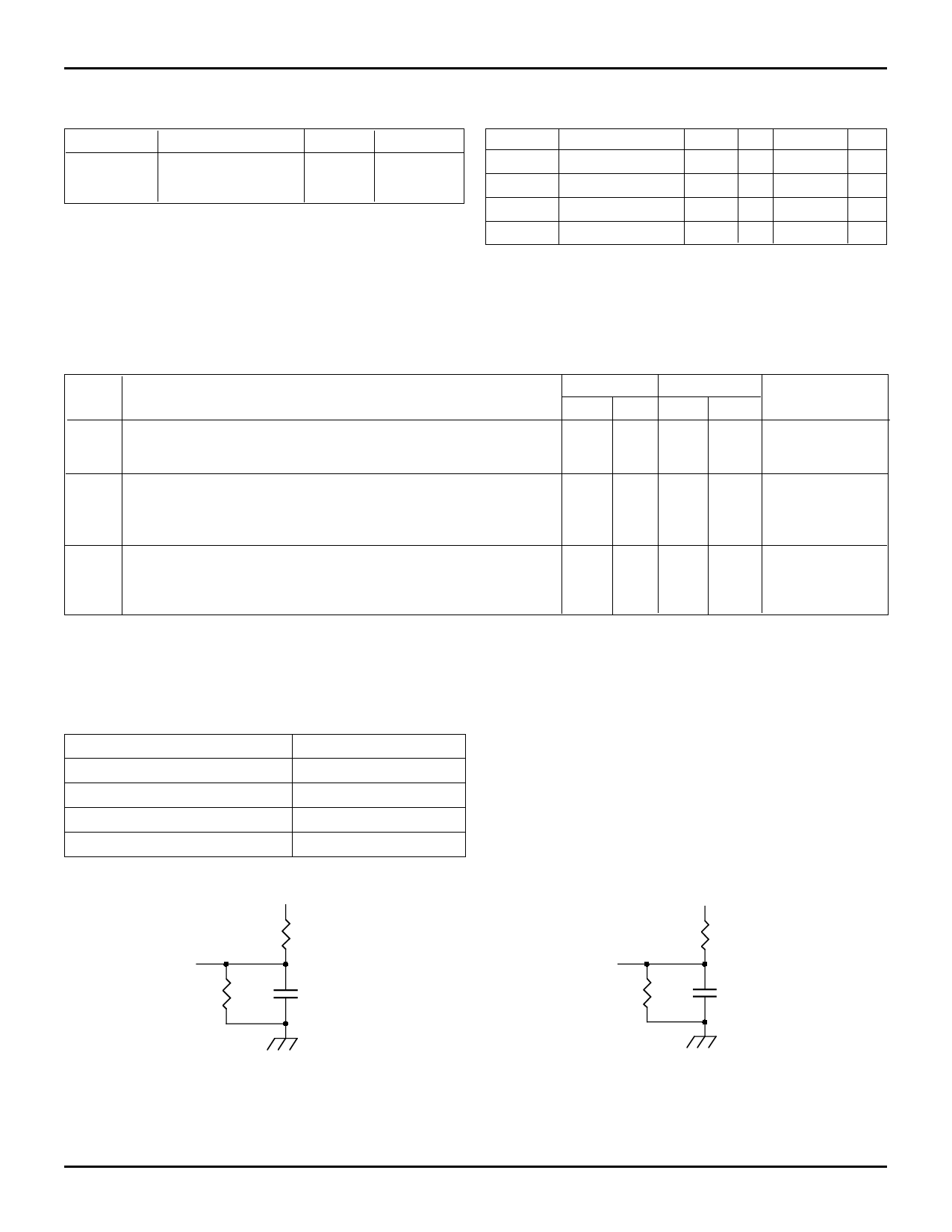
AC Test Conditions
Input Pulse Levels
Input Rise/Fall Times
Input Timing Reference Levels
Output Reference Levels
AC Test Load
GND to 3.0V
3ns
1.5V
1.5V
See Figures 1 and 2
2971 tbl 08
5V
5V
DATA OUT
255Ω
480Ω
30pF*
,
2971 drw 03
DATA OUT
255Ω
480Ω
5pF*
,
2971 drw 04
Figure 1. AC Test Load
*Includes scope and jig capacitances
Figure 2. AC Test Load
(for tCLZ, tOLZ, tCHZ, tOHZ, tOW, tWHZ)
6.432
Share Link: 