42744V33 View Datasheet(PDF) - Infineon Technologies
Part Name
Description
View to exact match
42744V33 Datasheet PDF : 18 Pages
| |||
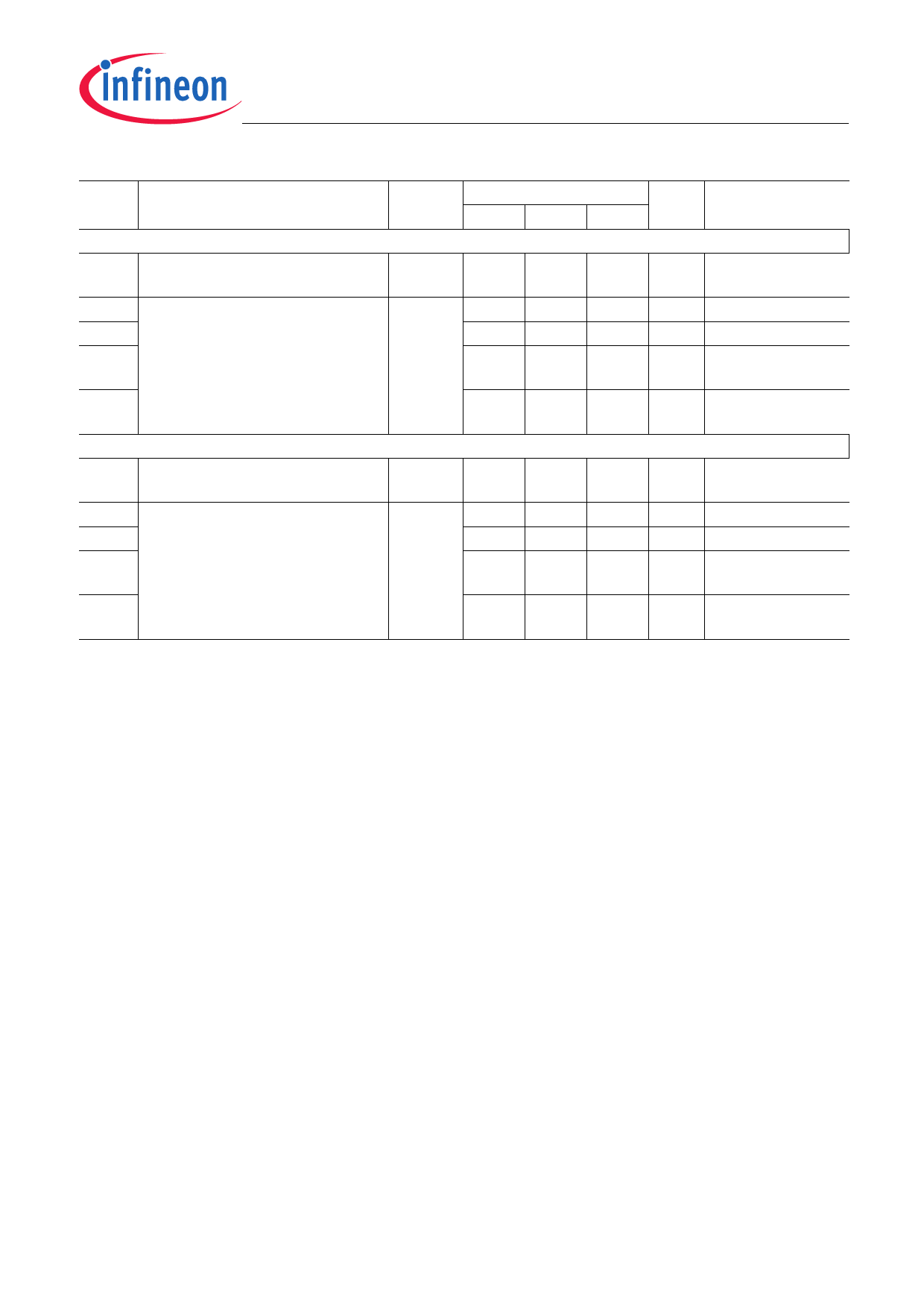
TLE42744
General Product Characteristics
Pos. Parameter
Symbol
Limit Values
Unit Conditions
Min. Typ. Max.
TLE42744EV50 (PG-SSOP-14 exposed pad)
4.3.11 Junction to Case1)
RthJC
–
4.3.12 Junction to Ambient1)
4.3.13
RthJA
–
–
7
–
43
–
120 –
K/W measured to
exposed pad
K/W 2)
K/W footprint only3)
4.3.14
–
59
–
K/W 300 mm² heatsink
area3)
4.3.15
–
49
–
K/W 600 mm² heatsink
area3)
TLE42744GSV33 (PG-SOT223-4)
4.3.16 Junction to Case1)
RthJC
–
17
–
K/W measured to heat
slug
4.3.17 Junction to Ambient1)
4.3.18
RthJA
–
–
54
–
139 –
K/W
K/W
2)
footprint only3)
4.3.19
–
73
–
K/W 300 mm² heatsink
area3)
4.3.20
–
64
–
K/W 600 mm² heatsink
area3)
1) Not subject to production test, specified by design.
2) Specified RthJA value is according to Jedec JESD51-2,-5,-7 at natural convection on FR4 2s2p board; The Product
(Chip+Package) was simulated on a 76.2 x 114.3 x 1.5 mm³ board with 2 inner copper layers (2 x 70µm Cu, 2 x 35µm Cu).
Where applicable a thermal via array under the exposed pad contacted the first inner copper layer.
3) Specified RthJA value is according to Jedec JESD 51-3 at natural convection on FR4 1s0p board; The Product
(Chip+Package) was simulated on a 76.2 × 114.3 × 1.5 mm3 board with 1 copper layer (1 x 70µm Cu).
Data Sheet
8
Rev. 1.1, 2010-01-13
Share Link: 