TC58NVG1S3BFT00 View Datasheet(PDF) - Toshiba
Part Name
Description
View to exact match
TC58NVG1S3BFT00 Datasheet PDF : 37 Pages
| |||
TC58NVG1S3BFT00/TC58NVG1S8BFT00
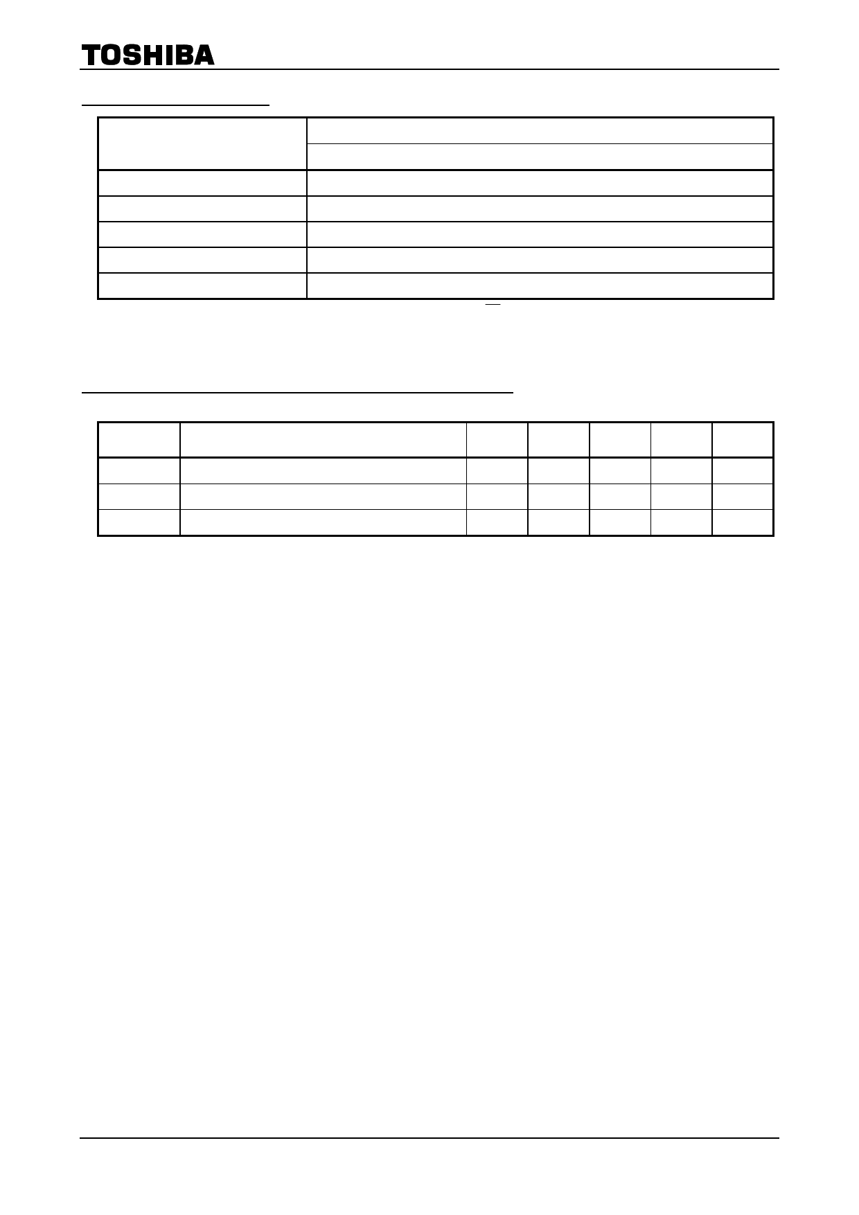
AC TEST CONDITIONS
PARAMETER
CONDITION
2.7 V ≤ VCC ≤ 3.6 V
Input level
2.4 V, 0.4 V
Input pulse rise and fall time
3ns
Input comparison level
1.5 V, 1.5 V
Output data comparison level
1.5 V, 1.5 V
Output load
CL (100 pF) + 1 TTL
Note: Busy to ready time depends on the pull-up resistor tied to the RY / BY pin.
(Refer to Application Note (9) toward the end of this document.)
PROGRAMMING AND ERASING CHARACTERISTICS
(Ta = 0 to 70℃, VCC = 2.7 V to 3.6 V)
SYMBOL
PARAMETER
MIN
tPROG
Average Programming Time
N
Number of Partial Program Cycles in the Same Page
tBERASE
Block Erasing Time
(1) Refer to Application Note (12) toward the end of this document.
TYP.
200
1.5
MAX
500
8
3
UNIT
µs
ms
NOTES
(1)
6
2003-10-30A
Share Link: 